LDMOS device and fabrication method thereof

A technology of devices and body regions, applied in semiconductor/solid-state device manufacturing, semiconductor devices, electrical components, etc., can solve problems such as high breakdown voltage, large on-resistance, and low on-resistance

Active Publication Date: 2012-03-21
CSMC TECH FAB2 CO LTD
View PDF5 Cites 10 Cited by
  • Summary
  • Abstract
  • Description
  • Claims
  • Application Information

AI Technical Summary

Problems solved by technology

[0004] In view of this, it is necessary to provide an LDMOS device with a higher breakdown voltage and a lower on-resistance in view of the problem that the LDMOS device withstands the withstand voltage by reducing the doping concentration of the drift region, resulting in a larger on-resistance.
[0005] In addition, it is also necessary to provide an LDMOS device with a higher breakdown voltage and a lower on-resistance in view of the problem that the LDMOS device withstands a withstand voltage by reducing the doping concentration of the drift region, resulting in a larger on-resistance. Manufacturing method

Method used


Image

  • LDMOS device and fabrication method thereof
  • LDMOS device and fabrication method thereof
  • LDMOS device and fabrication method thereof

Examples


Embodiment Construction

[0025] Based on the structure of the present invention, N-type LDMOS devices and P-type LDMOS devices can be realized. Taking N-type LDMOS as an example, if the P-type LDMOS device structure of the present invention is to be realized, those skilled in the art only need to follow the embodiment of the present invention Just make the corresponding changes.

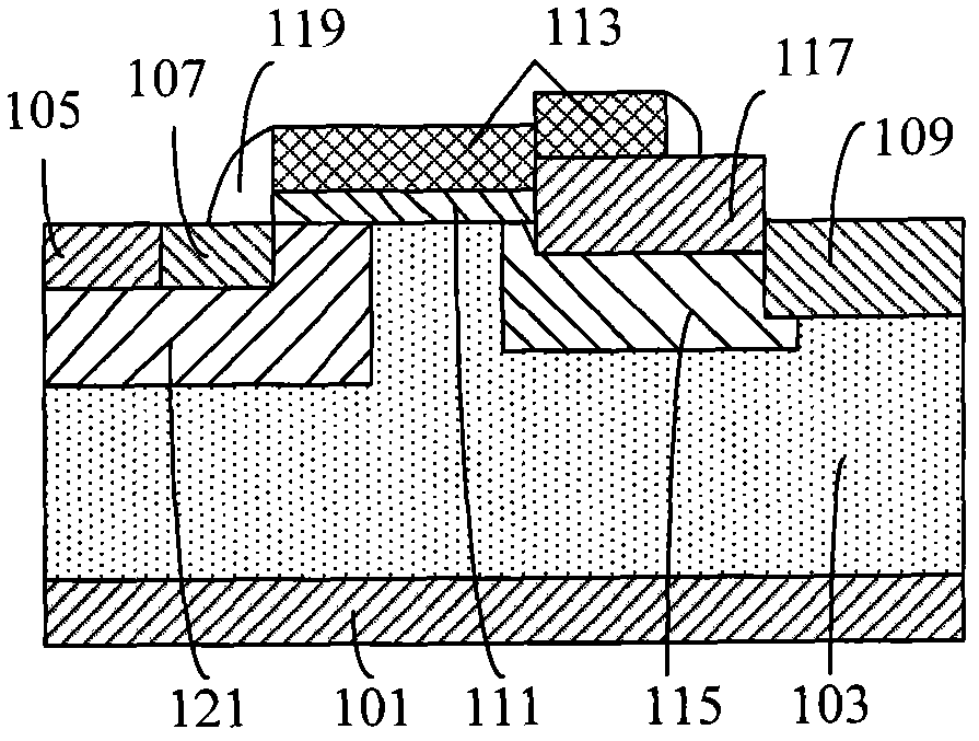
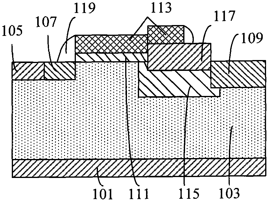
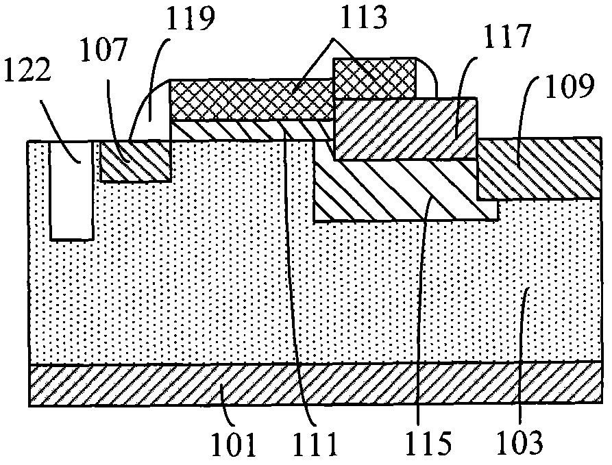
[0026] Such as figure 1 As shown, an LDMOS device includes a substrate 101, a body region 103 (P-well), a body region lead 105, a source region, a source region lead 107, a drain region, a drain region lead 109, a gate oxide layer 111, a gate Region 113 , drift region 115 , insulating dielectric layer 117 , gate sidewall regions 119 located on both sides of gate region 113 , and P-body region 121 .

[0027] The insulating dielectric layer 117 is located above the drift region 115 and below the gate region 113 . The insulating dielectric layer 117 is made of an electrically insulating material such as silicon dioxide. The ...


PUM


Abstract

The invention discloses a laterally diffused metal oxide semiconductor (LDMOS) device; the LDMOS device comprises a source region, a gate region, a drain region, a body region, and a drifting region with doped type opposite to the body region; the body region is arranged on a substrate region, and the drifting region is arranged between the drain region and the body region. The LDMOS device also comprises an insulated dielectric layer, and the insulated dielectric layer is positioned on the drifting region and below the gate region. By using the structure of the LDMOS device provided by the invention, the puncture voltage of the device can be enhanced, so that the on-resistance is lowered and the power consumption of the device is reduced; and in the adjusting and fabricating process, junction depth for adjusting the insulated dielectric layer and the drifting region has smaller effect on the other devices.

Description

【Technical field】 [0001] The invention relates to an LDMOS device and a manufacturing method thereof. 【Background technique】 [0002] The lateral double diffused MOS transistor (LDMOS) is a lightly doped drain MOS device. Since LDMOS generally works in the linear region, its current remains basically unchanged, so the power consumption of LDMOS mainly depends on the size of the on-resistance. To increase the breakdown voltage, there is a drift region between the active and drain regions. The drift region in LDMOS is the key to the design of this type of device. The impurity concentration in the drift region is relatively low. Therefore, when the LDMOS is connected to a high voltage, the drift region can withstand a higher voltage due to its high resistance. [0003] At present, the traditional device structure uses a drift region made of a deep well to withstand the device withstand voltage. Due to the deep well depth, it is difficult to deplete the drift region, so the do...

Claims


Application Information

Patent Timeline
Patent Type & Authority Applications(China)
IPC IPC(8): H01L29/06H01L21/336H01L29/78
CPCH01L29/1087H01L29/7835H01L29/42368
Inventor 吴孝嘉罗泽煌孙贵鹏
Owner CSMC TECH FAB2 CO LTD
Why Eureka
Try Eureka