Analog/digital configurable variable-gain amplifier

A gain amplifier and gain amplification technology, applied in the field of radio frequency communication, can solve the problems of discontinuity of VGA gain change, increase of module circuit complexity, deterioration of signal-to-noise ratio of radio frequency receiver system, etc.

Inactive Publication Date: 2012-03-21
杭州中科微电子有限公司
View PDF5 Cites 47 Cited by
  • Summary
  • Abstract
  • Description
  • Claims
  • Application Information

AI Technical Summary

Problems solved by technology

[0006] There are many disadvantages in the prior art controllable gain amplifier: first, the analog control gain amplifier or the digital control gain amplifier of the traditional structure can only be suitable for a kind of baseband chip, not suitable for sharing with different demodulation chips, and jointly integrating
Second, in the traditional design, the digital control gain amplifier and the analog control gain amplifier are two independent modules. When designing, the cascading of the two amplifiers with the front and rear stages and the matching and isolation between the front and rear stages should be considered. The switching of different working modes on the signal chain, as well as some special connection requirements, etc., not only increase the difficulty of design, but also increase the complexity of the module circuit
Third, the traditional circuit structure of two parallel chips greatly increases the chip area and makes it more difficult to cooperate with the baseband, which deteriorates the signal-to-noise ratio of the RF receiver system and ultimately affects system performance
Fourth, there is interference between different amplifiers in parallel, as well as substrate noise problems, which seriously restrict the performance of the entire system and high-demand applications
Programmable makes the control more flexible and can achieve the required characteristics more easily, but it also has a digital feedback control signal that will cause the discontinuity of the VGA gain change and the discontinuity of the signal phase, and the discontinuous change of the gain limits the its purpose

Method used


Image

  • Analog/digital configurable variable-gain amplifier
  • Analog/digital configurable variable-gain amplifier
  • Analog/digital configurable variable-gain amplifier

Examples


no. 1 example

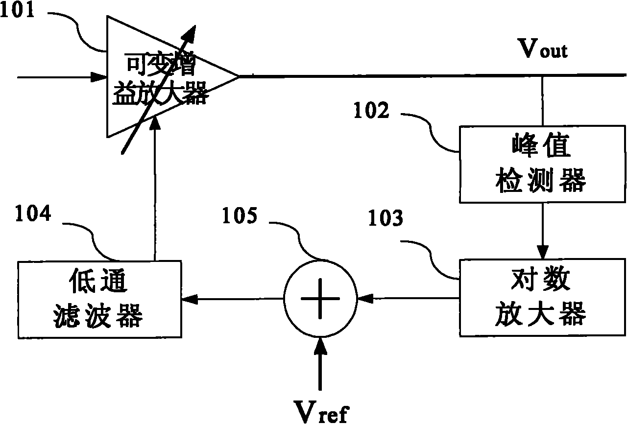
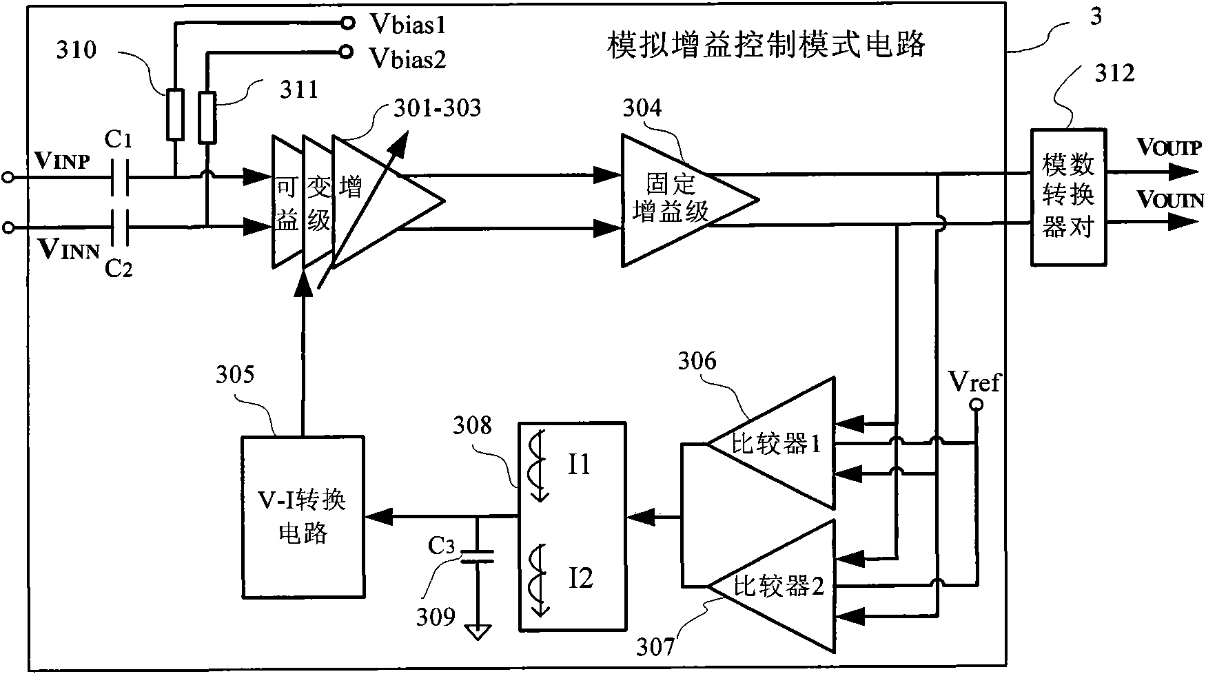
[0072] image 3 A block diagram of the circuit configuration of the analog control mode of the variable gain amplifier of the embodiment of the present invention is given. combine image 3 Explain that the analog control mode in the present invention realizes the composition: the input signal V INP and V INN Enter the differential input terminal of the variable gain amplifier, the variable gain stages 301 to 303 of the three stages of the variable gain amplifier are connected in cascade, the two differential outputs of 303 are connected to the differential input terminal of the fixed gain amplifier 304, and the output of the fixed gain stage 304 The two differential signals pass through the differential comparator pair 306 and 307 with the set reference voltage V ref For comparison, the differential outputs of comparators 306 and 307 pass through charge pump circuit 308 to C 3 Capacitor 309 is charged or discharged so that it outputs a suitable control voltage to the input...

no. 2 example

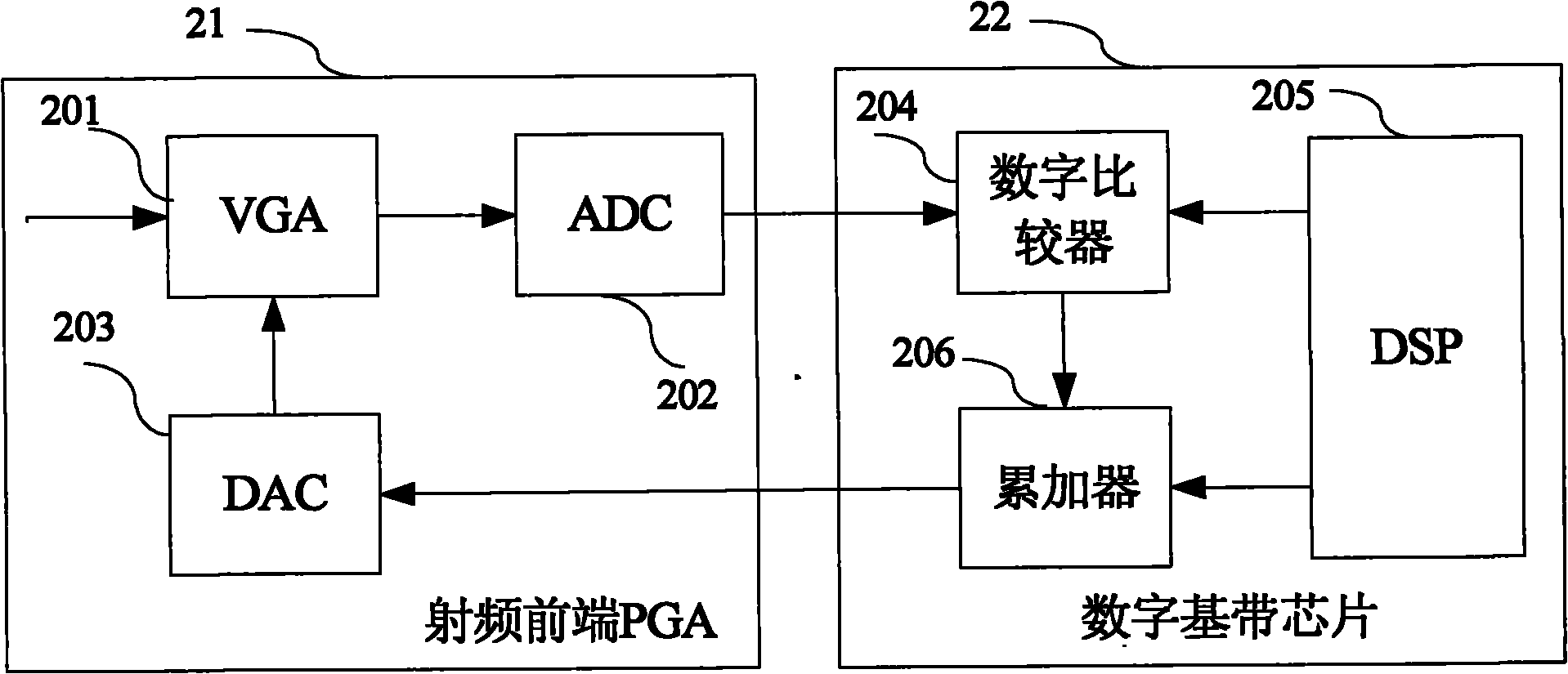
[0074] Figure 4 A block diagram of a variable gain amplifier circuit configured with analog and digital control modes in an application embodiment of the present invention is given. Block diagram of variable gain amplifier circuit configured in analog control mode and image 3 The given block diagrams of the circuits in the analog control mode of the variable gain amplifier in the embodiment of the present invention are the same. The configuration of the analog and digital control modes is controlled by the control circuit 414 by the receiver control signal 417 to realize mode switching. The receiver control signal 417 is connected to the corresponding control port of the control circuit 41, and the output terminal of the control circuit 41 is connected to the digital-to-analog converter. The input terminal of 413, the output terminal of the digital-to-analog converter 413 is added to an input terminal of the I-V conversion circuit. If the receiver configuration is selected...

no. 3 example

[0077] Figure 5 Provide the RF module front-end digital / analog configurable variable gain intermediate frequency amplifier of the second application embodiment of the present invention, Figure 5 Only a schematic block diagram of a front-end signal of a differential RF module and a configurable intermediate frequency amplifier is given in . The front-end signal of the radio frequency module enters the main amplifier 501-503 and amplifies step by step. The gain control terminal of each amplifier is connected to the control output terminal of the V-I conversion control circuit 505. The gain of each amplifier is controlled by the output signal of the control circuit 505. The gain control mode is selected through the baseband chip 52 in cooperation with the receiver control signal. If the analog control mode is selected, the receiver control signal is switched to terminal 2 through the switch circuit 506, and the analog control mode is the same as image 3 The circuit compositi...


PUM


Abstract

The invention discloses an analog / digital configurable variable-gain amplifier, which comprises a variable-gain amplifier module VGA and an analog / digital configurable control circuit. The variable-gain amplifier module is formed by a plurality of variable-gain amplifiers and a fixed-gain amplifier in concatenation connection. The analog / digital configurable control circuit comprises an analog mode control circuit and a digital mode control circuit. A comparator and a charge pump of the analog mode control circuit detect the size of amplitude of an output signal, output an appropriate control voltage and feed back the control voltage to the VGA so as to regulate the gain of the VGA. The digital mode control circuit controls an internal switch circuit by means of an external signal, generates the control voltage by means of a decoder and an I-V converter according to an input signal provided by a digital baseband processing module chip and feeds back the control voltage to the VGA so as to change the gain of the VGA. The analog / digital configurable variable-gain amplifier can flexibly switch between an analog mode and a digital mode and is especially suitable for a radio-frequency front end circuit for different baseband chips.

Description

Contents of the invention [0001] The invention belongs to the technical field of radio frequency communication, and relates to a variable gain amplifier, in particular to an analog / digital configurable variable amplifier used in a radio frequency receiver, which can work in either an analog control mode or a digital Control mode, the switching between the two modes is realized through external control signals. Background technique [0002] In recent years, with the continuous emergence of new technologies in the field of information technology and the continuous progress of technology, the RF front-end and baseband chips of various receiver systems have achieved great development. The development of chips with a single function is becoming more and more mature, but because of its single function, people turn their attention to the development of chips with multiple functions, including multi-function chips that support multiple operating frequency bands and multi-functional ...

Claims


Application Information

Patent Timeline
Patent Type & Authority Applications(China)
IPC IPC(8): H03G3/20
Inventor 何晓丰莫太山马成炎
Owner 杭州中科微电子有限公司
Why Eureka
Try Eureka