Vertical type PNP triode in SiGe BiCMOS process and manufacturing method thereof

A PNP triode, vertical technology, applied in semiconductor/solid-state device manufacturing, electrical components, circuits, etc., can solve the problems of large width, wide base area, etc., to improve the characteristic frequency, expand the application field, and improve design flexibility Effect

Active Publication Date: 2012-04-11
SHANGHAI HUAHONG GRACE SEMICON MFG CORP
View PDF5 Cites 7 Cited by
  • Summary
  • Abstract
  • Description
  • Claims
  • Application Information

AI Technical Summary

Problems solved by technology

[0007] Due to the consideration of the breakdown voltage and process repeatability of the existing PNP transistor, the base area width is relatively wide
In addition, the collector region of the existing PNP transistor is formed by P well technology, and the emitter region is formed by ion implantation. The combination makes the emitter region, the base region and the collector region very wide, and the emitter-base depletion region, base-collector The width of the depletion region is also large

Method used


Image

  • Vertical type PNP triode in SiGe BiCMOS process and manufacturing method thereof
  • Vertical type PNP triode in SiGe BiCMOS process and manufacturing method thereof
  • Vertical type PNP triode in SiGe BiCMOS process and manufacturing method thereof

Examples


Embodiment Construction

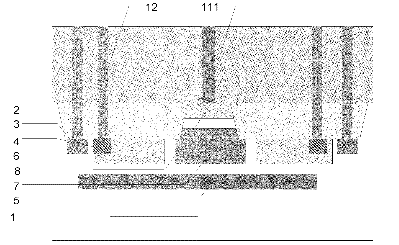
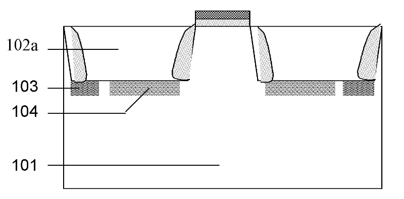
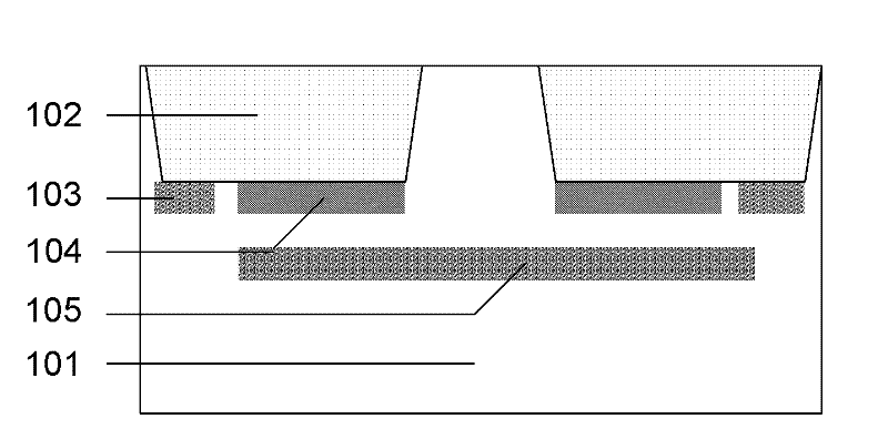
[0030] like Figure 2H As shown, it is a schematic diagram of a vertical PNP transistor in the SiGe BiCMOS process of the embodiment of the present invention. The vertical PNP transistor in the SiGe BiCMOS process of the embodiment of the present invention is formed on a P-type silicon substrate 101, and the active region passes through a shallow groove. Field oxygen 102 isolation, the vertical PNP transistor includes:

[0031] A collector region is composed of a first P-type impurity region 106 and a P-type pseudo-buried layer 104; the P-type pseudo-buried layer 104 is formed at the bottom of the shallow trench field oxygen 102 on both sides of the active region, so The width of the P-type pseudo-buried layer 104 is smaller than the width of the bottom of the shallow trench field oxygen 102; the first P-type impurity region 106 is formed in the active region, and the depth of the first P-type impurity region 106 is greater than The depth of the shallow trench field oxygen 10...


PUM


Abstract

The invention discloses a vertical type PNP triode in a SiGe BiCMOS process and a manufacturing method thereof. The vertical type PNP triode comprises a collector region, an outer isolation region, a base region, and an emission region. The collector region is composed of first P type impurity regions and P type burying layers; the P type burying layers are formed at shallow groove field oxygen bottoms that are at two sides of an active area as well as are adjoined with the active area; deep hole contacts are formed at the tops of the P type burying layers so as to lead out collectors. The outer isolation region includes N type burying layers that formed at the shallow groove field oxygen bottoms that are at the two sides of the active area; and there are lateral separations between the N type burying layers and the P type burying layers. The base region comprises an intrinsic base region and an outer base region. The intrinsic base region is formed by an N type silicon epitaxial layer that is formed at the upper portion of the active area. The emission region is formed by a P type SiGe epitaxial layer and a polysilicon layer, wherein the P type SiGe epitaxial layer is formed on the intrinsic base region. In addition, the invention also discloses a manufacturing method of the vertical type PNP triode in the SiGe BiCMOS process. According to the invention, a characteristic frequency of the PNP triode can be improved; the PNP triode can be integrated into a current process; flexibilities of the PNP triode design can be improved.

Description

technical field [0001] The invention relates to the field of semiconductor integrated circuit manufacturing, in particular to a vertical PNP transistor in a silicon-germanium BiCMOS process, and also relates to a manufacturing method for a vertical PNP transistor in a silicon-germanium BiCMOS process. Background technique [0002] In the silicon germanium BiCMOS process, the cut-off frequency and breakdown voltage of the NPN triode, that is, the N-type tube, have been made very high, but the performance of the PNP triode, that is, the P-type tube, is poor. Most of the existing P-type tubes adopt a parasitic transverse structure. like figure 1 As shown, it is a PNP transistor in the existing SiGe BiCMOS process, which is formed on a P-type silicon substrate 1, and the active region is isolated by a shallow trench field oxygen 2. The PNP transistor includes: [0003] A collector region is composed of a P well 6 and a P-type pseudo-buried layer 4, the P well 6 is formed at th...

Claims


Application Information

Patent Timeline
Patent Type & Authority Applications(China)
IPC IPC(8): H01L29/732H01L21/331H01L21/265
Inventor 周正良季伟
Owner SHANGHAI HUAHONG GRACE SEMICON MFG CORP
Why Eureka
Try Eureka