Manufacturing method of multi-frequency CMUT device and multi-frequency CMUT device

A manufacturing method and device technology, which are applied in piezoelectric devices/electrostrictive devices, manufacturing microstructure devices, piezoelectric/electrostrictive/magnetostrictive devices, etc., can solve problems such as complex production processes and reduce manufacturing Cost, the effect of reducing the difficulty of manufacturing

Active Publication Date: 2020-08-21
NEIJIANG NORMAL UNIV +1
View PDF16 Cites 1 Cited by
  • Summary
  • Abstract
  • Description
  • Claims
  • Application Information

AI Technical Summary

Problems solved by technology

However, methods such as adjusting the radius of the film, increasing the thickness of the film, and changing the material of the film need to adjust the layout of at least two layers of design layout, and the production process is more complicated.

Method used


Image

  • Manufacturing method of multi-frequency CMUT device and multi-frequency CMUT device
  • Manufacturing method of multi-frequency CMUT device and multi-frequency CMUT device
  • Manufacturing method of multi-frequency CMUT device and multi-frequency CMUT device

Examples


Embodiment Construction

[0029] The technical solutions in the embodiments of the present application will be described below in conjunction with the drawings in the embodiments of the present application.

[0030] It should be noted that similar reference numerals and letters indicate similar items in the following drawings. Therefore, once an item is defined in one drawing, it does not need to be further defined and explained in the subsequent drawings. At the same time, in the description of this application, the terms "first", "second", etc. are only used to distinguish the description, and cannot be understood as indicating or implying relative importance.

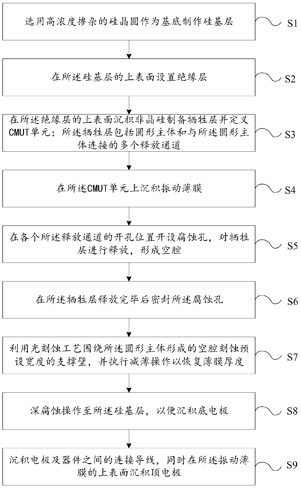
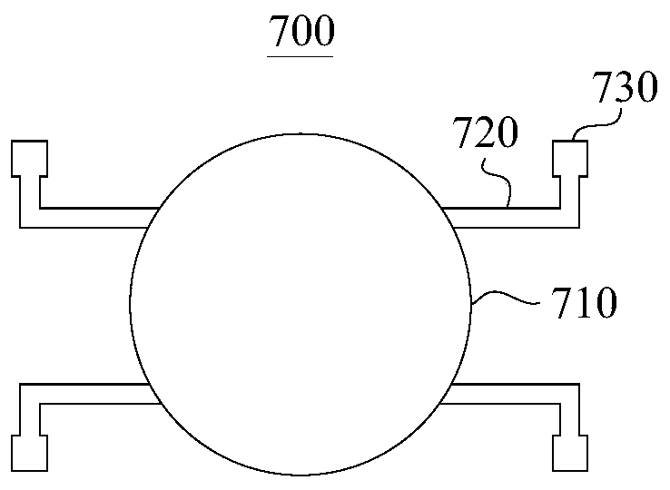
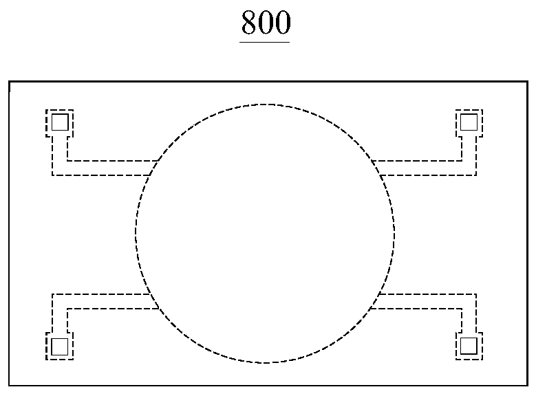
[0031] Please see figure 1 , figure 2 , image 3 with Figure 4 , figure 1 A schematic flow chart of a manufacturing method of a multi-frequency CMUT device provided by an embodiment of this application; figure 2 A schematic diagram of the first layer mask structure when manufacturing a multi-frequency CMUT device provided by an embodiment of thi...


PUM


Abstract

The invention provides a manufacturing method of a multi-frequency CMUT device and the multi-frequency CMUT device. The method comprises the steps: selecting a high-concentration doped silicon wafer as a substrate to manufacture a silicon-based layer; arranging an insulating layer on the upper surface of the silicon-based layer; depositing amorphous silicon on the upper surface of the insulating layer to prepare a sacrificial layer and define a CMUT unit, wherein the sacrificial layer comprises a circular main body and a plurality of release channels connected with the circular main body; depositing a vibration film on the CMUT unit; forming a corrosion hole in the opening position of each release channel, and releasing the sacrificial layer to form a cavity; sealing the corrosion hole after the sacrificial layer is released; etching a supporting wall with a preset width around a cavity formed by the circular main body by using a photoetching process; performing a deep etching operation to the silicon-based layer so as to deposit a bottom electrode; and depositing a connecting wire between the electrode and a device, and depositing a top electrode on the upper surface of the vibration film.

Description

Technical field [0001] This application relates to the technical field of ultrasonic sensor manufacturing, in particular to a method for manufacturing a multi-frequency CMUT device and a multi-frequency CMUT device. Background technique [0002] Ultrasound probes play a key role in ultrasonic imaging; ultrasonic sensors are the key components of ultrasonic probes. Early ultrasonic sensors generally used lead zirconate titanate ceramics (PZT). With the development of technology, capacitive micromachined ultrasonic The sensor (CMUT) has the advantage of replacing it because of its wide frequency bandwidth, easy integration of integrated circuits, and easy processing. The intrinsic frequency of the CMUT can determine the accuracy of imaging. Generally, methods to increase the intrinsic frequency of the CMUT include reducing the film radius, increasing the film thickness, and changing the film material. However, methods such as adjusting the film radius, increasing the film thicknes...

Claims


Application Information

Patent Timeline
Patent Type & Authority Applications(China)
IPC IPC(8): B81B3/00B81C1/00
CPCB81B3/0018B81C1/00134B81C1/00158B81B2201/0292
Inventor 王久江余远昱旷江明徐晶杨济宁张双李尧刘益和
Owner NEIJIANG NORMAL UNIV
Why Eureka
Try Eureka