Gallium nitride based light emitting diode and manufacturing method thereof

A light-emitting diode, gallium nitride-based technology, applied in the direction of electrical components, circuits, semiconductor devices, etc., can solve the problems of uneven distribution, inability to fully utilize the light-emitting area of ​​the active layer, and affect the light-taking efficiency of light-emitting diodes, so as to improve The effect of luminous efficiency

Inactive Publication Date: 2012-04-18
XIAMEN SANAN OPTOELECTRONICS TECH CO LTD
View PDF4 Cites 13 Cited by
  • Summary
  • Abstract
  • Description
  • Claims
  • Application Information

AI Technical Summary

Problems solved by technology

Since the electrode has only a small part of the contact with the epitaxial light-emitting stack, the current is easily confined to the area of ​​the contacted part, causing the current to flow from the electrode into the active layer in the epitaxial light-emitting stack, only co

Method used


Image

  • Gallium nitride based light emitting diode and manufacturing method thereof
  • Gallium nitride based light emitting diode and manufacturing method thereof
  • Gallium nitride based light emitting diode and manufacturing method thereof

Examples


Example Embodiment

[0032] Example 1

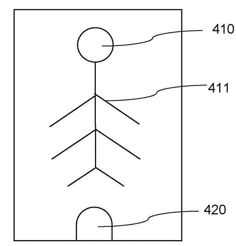
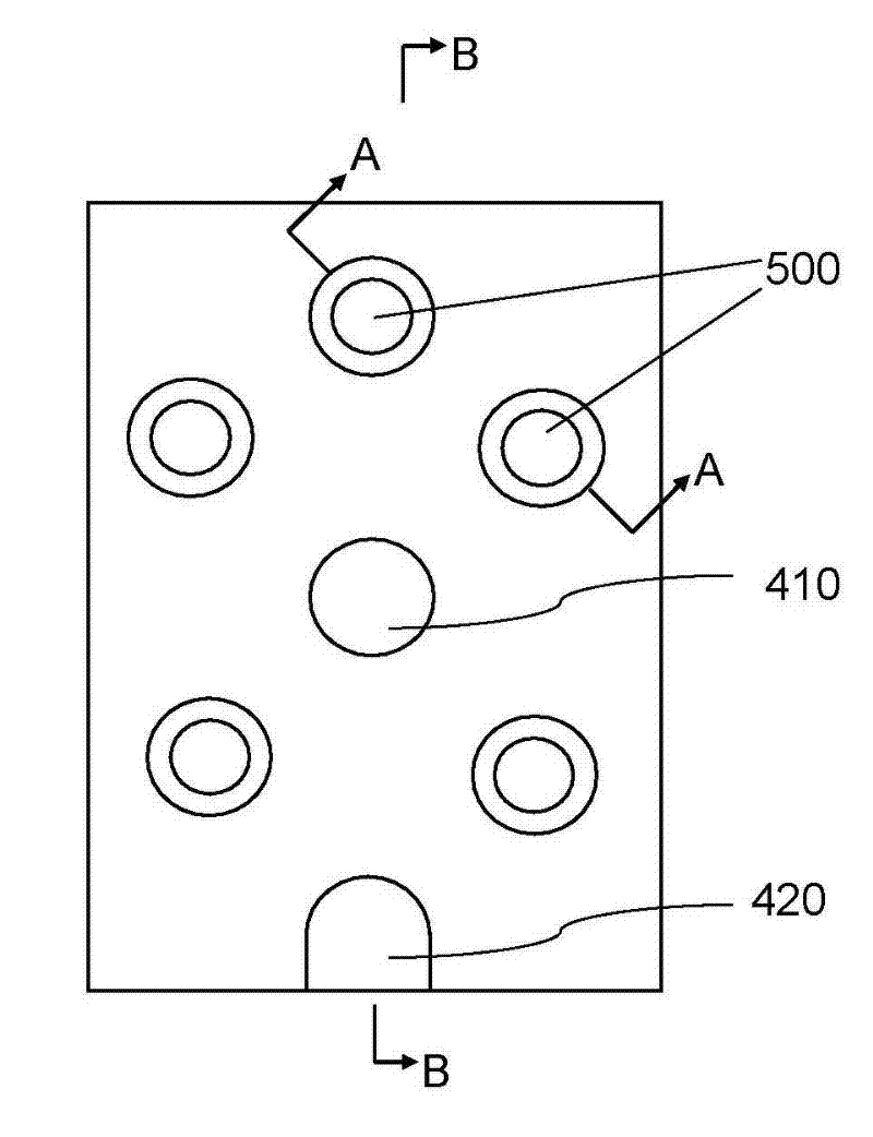
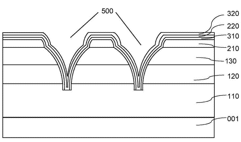
[0033] Such as Figure 4 As shown, a gallium nitride-based light-emitting diode includes: a substrate 001, a semiconductor epitaxial layer is deposited on the substrate 001, which includes an n-type semiconductor layer 110, an active layer 120, and a p-type semiconductor layer 130 from bottom to top The first transparent current spreading layer 210 is formed on the p-type semiconductor layer 130; the first electrode 410 is formed on the first transparent current spreading layer 210 and is located in the central area of ​​the epitaxial layer; the series of holes 500 are distributed in the first electrode 410 It penetrates the p-type semiconductor layer 130 and the active layer 120, and the bottom is located on the n-type semiconductor layer 110; the first insulating layer 310 is formed on the first transparent current spreading layer 210 and extends to the sidewall of the hole 500 to cover the first A transparent current spreading layer 210 and the sidewalls of...

Example Embodiment

[0039] Example 2

[0040] Figure 5~Figure 13 It is a cross-sectional view of a manufacturing process of a gallium nitride-based light emitting diode according to an embodiment of the present invention. The manufacturing process mainly includes an epitaxial growth step, a first transparent current spreading layer forming step, a patterning a first transparent current spreading layer step, a hole forming step, a first transparent current spreading layer forming step, and an electrode manufacturing step. A detailed description will be given below in conjunction with the drawings.

[0041] First, a substrate 001 is provided, and a light-emitting epitaxial layer is deposited on the substrate, which includes an n-type semiconductor layer 110, an active layer 120, and a p-type semiconductor layer 130 from bottom to top. The substrate is an insulating material, and common materials such as sapphire, silicon, and silicon carbide can be used. The deposition of the light-emitting epitaxia...


PUM


Abstract

The invention discloses a gallium nitride based light emitting diode and a manufacturing method thereof. In the invention, a double-layer transparent conducting layer structure is designed, a first transparent extension layer is formed on a p type semiconductor layer, a p electrode is provided at a center area of an epitaxial structure layer, peripheral of the p electrode is provided with a hole structure, and a second transparent extension layer is formed in the hole structure and is connected with an n electrode to form an equipotential surface. After current is injected from the p electrode, the current diffuses to a whole light emitting surface through the first transparent extension layer and flows to an n type layer through the p type semiconductor layer, and since the second transparent extension layer and the n electrode are in a same electric potential, the current diffuses to the second transparent extension layer to reach the n electrode finally. According to the gallium nitride based light emitting diode and the manufacturing method, in a process that the current flows to the n electrode from the p electrode, the current is uniformly distributed on an epitaxial luminescent layer, a current flow through path of a P layer is shorter, simultaneously, structure of partial light emitting surface is changed, and luminescence efficiency is effectively raised.

Description

technical field [0001] The invention relates to a gallium nitride-based light-emitting diode and a manufacturing method thereof, in particular to a gallium-nitride-based light-emitting diode with double transparent current spreading layers and a manufacturing method thereof. Background technique [0002] In recent years, the development of semiconductor lighting technology represented by gallium nitride-based wide-bandgap semiconductor materials has attracted worldwide attention. With the continuous improvement of epitaxy and chip process technology, the luminous efficiency of gallium nitride-based light-emitting diodes has been continuously improved. However, in order to popularize semiconductor lighting in a real sense, it still needs to continue to improve on the existing level of light efficiency. The light efficiency of light-emitting diodes mainly depends on the internal quantum efficiency and light extraction efficiency. The former is determined by the epitaxial crys...

Claims


Application Information

Patent Timeline
IPC IPC(8): H01L33/14H01L33/38H01L33/00
Inventor 欧毅德尹灵峰刘传桂林素慧
Owner XIAMEN SANAN OPTOELECTRONICS TECH CO LTD
Why Eureka
Try Eureka