Tunnel diodes made of stress-compensated compound semiconductor layers

A technology of tunnel diodes and semiconductors, applied in the field of solar cells, can solve the problems that tunnel diodes should not absorb light and reduce the efficiency of solar cells.

Active Publication Date: 2012-04-18
FRAUNHOFER GESELLSCHAFT ZUR FOERDERUNG DER ANGEWANDTEN FORSCHUNG EV
View PDF1 Cites 9 Cited by
  • Summary
  • Abstract
  • Description
  • Claims
  • Application Information

AI Technical Summary

Problems solved by technology

Crystalline defects in the layers typically form recombination centers for photogenerated charge carriers, reducing the efficiency of solar cells
In addition, the tunnel diodes used in the part of the cell underneath which are also used for photovoltaic energy conversion should not absorb light

Method used


Image

  • Tunnel diodes made of stress-compensated compound semiconductor layers
  • Tunnel diodes made of stress-compensated compound semiconductor layers
  • Tunnel diodes made of stress-compensated compound semiconductor layers

Examples


Embodiment Construction

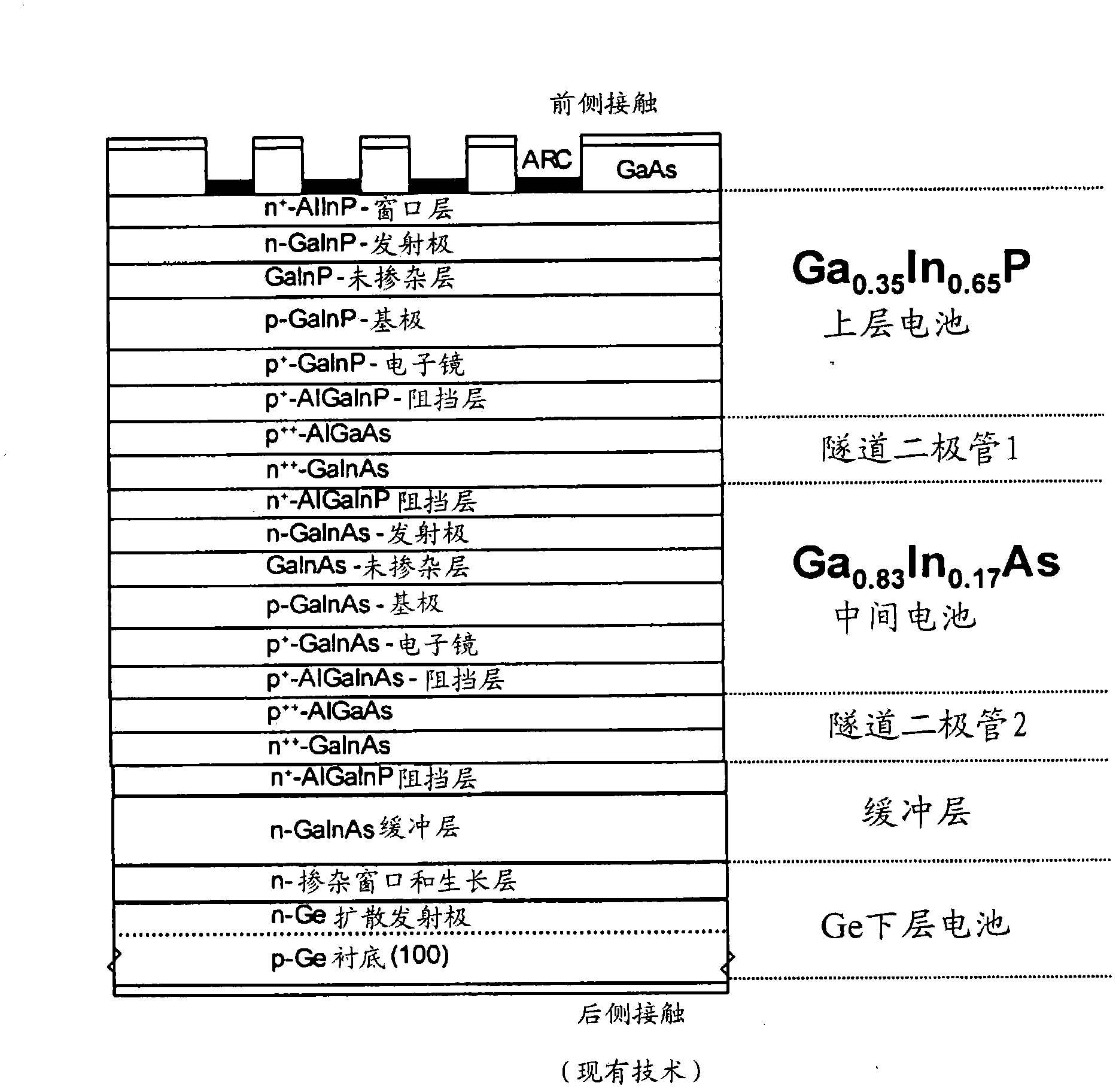
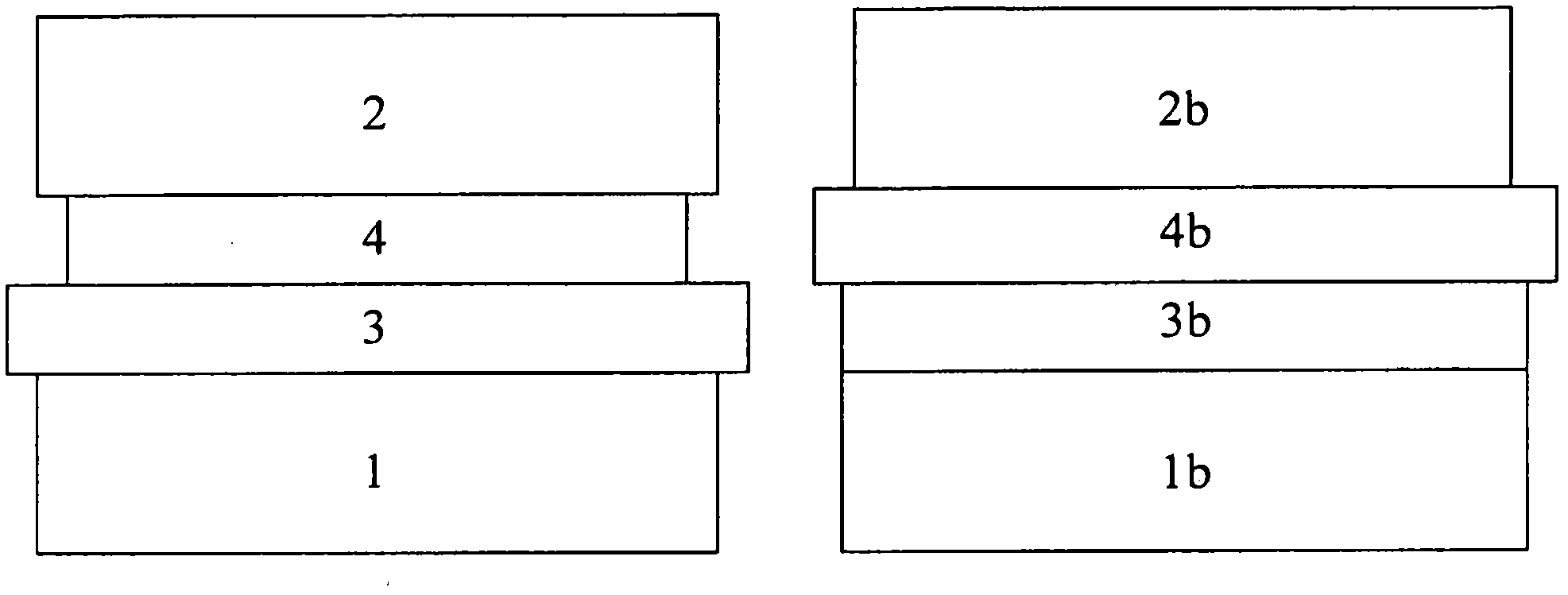
[0050] figure 2 Two layer sequences according to the invention are shown, comprising two semiconductor layers 1 and 2 between which two layers 3 and 4 of a tunnel diode in the form of a sandwich. The different widths of the individual layers represented in the figure thus represent the original lattice constants of the materials used for each layer respectively. in accordance with figure 2 In the left-hand embodiment of the semiconductor component of the invention, the material of layer 3 thus has a larger lattice constant (subject to compressive stress) relative to layer 1, while the material of layer 4 has a smaller lattice constant than that of material 3 constant (subject to tensile stress). The material of layer 2 has a lattice constant approximately equal in size to the material used for layer 1 . exist figure 2 In the case of the semiconductor component of the example on the left, layer 3 is thus laminated on layer 1 and layer 4 is laminated on layer 3 . As a re...


PUM


Abstract

The invention relates to semiconductor components, particularly solar cells made of III-V compound semiconductors, as used in terrestrial PV concentrator systems or for the electrical power supply in satellites. It is also used in other optoelectronic components, such as laser and light emitting diodes, where either high tunnel current densities are required or special materials are used, and where stress of the overall structure is not desirable. The invention consists of forming tunnel diodes from semiconductor components made of stress-compensated semiconductor layers.

Description

technical field [0001] The invention relates to semiconductor elements, in particular solar cells made of III-V compound semiconductors, as used in terrestrial PV concentrator systems or for electrical energy supply in satellites. However, it is also used in other optoelectronic components, such as laser diodes and light emitting diodes, where high tunneling current densities are necessary, or where special materials are used, and where stresses in the overall structure are not required. Background technique [0002] Multiple solar cells consist of multiple p-n junctions comprising different semiconductor materials with reduced bandgaps. The semiconductor materials used are typically III-V compound semiconductors such as gallium arsenide and elementary semiconductors such as silicon or germanium. However, II-VI compound semiconductors such as cadmium telluride, mixed semiconductors such as silicon germanium (SiGe) may also be used. Multiple solar cells use a better solar s...

Claims


Application Information

Patent Timeline
Patent Type & Authority Applications(China)
IPC IPC(8): H01L33/06H01L31/0687H01L33/30
CPCH01L29/885H01S5/183H01L33/0045H01L33/30Y02E10/544H01L31/0687H01S5/3095Y02E10/50H01L33/06Y02E10/547Y02P70/50
Inventor 沃尔夫冈·古特弗兰克·迪姆罗特扬·朔内
Owner FRAUNHOFER GESELLSCHAFT ZUR FOERDERUNG DER ANGEWANDTEN FORSCHUNG EV
Why Eureka
Try Eureka