Method for manufacturing aluminum liner of double-layer passivation protection layer

A technology of passivation protective layer and manufacturing method, which is applied in the field of aluminum pad manufacturing, can solve problems such as difficult removal of titanium/titanium nitride anti-reflective layer, soft failure of chips, increase of contact resistance of aluminum pad, etc., to achieve filling Effect of smoothness, less residue, and improved filling ability

Inactive Publication Date: 2012-05-09
SHANGHAI HUALI MICROELECTRONICS CORP
View PDF2 Cites 13 Cited by
  • Summary
  • Abstract
  • Description
  • Claims
  • Application Information

AI Technical Summary

Problems solved by technology

However, if there is a depression in the aluminum filling shape, the titanium/titanium nitride anti-reflection layer in the depression will be difficult to remove,

Method used


Image

  • Method for manufacturing aluminum liner of double-layer passivation protection layer
  • Method for manufacturing aluminum liner of double-layer passivation protection layer
  • Method for manufacturing aluminum liner of double-layer passivation protection layer

Examples


Embodiment Construction

[0028] The present invention will be further described below in combination with principle diagrams and specific operation examples.

[0029] The passivation protection layer and the aluminum pad layer are the final steps in the manufacture of semiconductor chips. In industrial production, according to the requirements of the actual application environment, there are different options for single passivation protection layer or double passivation protection layer. The present invention relates to the case of a single passivation protection layer.

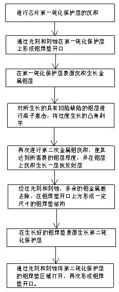
[0030] Such as figure 1 As shown, the manufacturing method of the aluminum liner of the double passivation protection layer of the present invention specifically comprises the following steps:

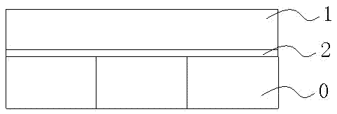
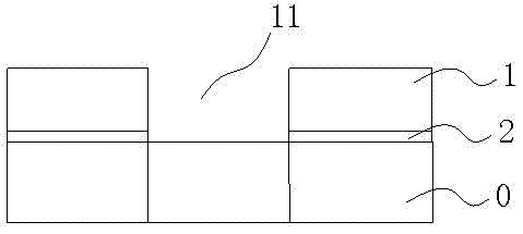
[0031] first step, such as Figure 2a As shown, the deposition of the first passivation protection layer of the chip is carried out. A first passivation protection layer 1 with a certain thickness is grown on the chip substrate 0 with int...


PUM


Abstract

The invention discloses a method for manufacturing an aluminum liner of a double-layer passivation protection layer. The method comprises the following steps of: depositing a first passivation protection layer of a chip; photoetching and etching the first passivation protection layer to form an aluminum weld pad opening; depositing a growth metal aluminum layer on the surface of the first passivation protection layer; ion bombardment the growth aluminum layer for scappling overgrowth convex angles; carrying out second metal aluminum deposition; photoetching and etching to form an aluminum weld pad structure above the aluminum weld pad opening; growing a second passivation protection layer on the surface of a grown aluminum weld pad; and photoetching and etching for opening an aluminum weld pad area of the second passivation protection layer to form the aluminum weld pad opening again. With the adoption of the process flow and the method and the utilization of plasma bombardment sputtering back etching and the multiple metal aluminum filling process, the filling capacity of aluminum is effectively improved, the filling of the edge area of contact holes is smoother, and the aluminum weld pad is smooth, does have a groove and has fewer defects, fewer remaining, low contact resistance and high the package reliability.

Description

technical field [0001] The invention relates to a semiconductor manufacturing technology, in particular to a method for manufacturing an aluminum pad of a double-layer passivation protection layer. Background technique [0002] In the semiconductor integrated circuit industry, high-performance integrated circuit chips require as low a defect as possible, high performance and highly reliable electrical connections, and the aluminum pad layer is the most surface interconnection of semiconductor integrated chips, directly in contact with the external environment , and it is a bridge connecting the chip and the peripheral circuit, which plays a very important role. Due to direct contact with the external environment, if the quality is poor, defects and failures will easily occur. During the packaging process, a large part of the failures comes from excessive contact resistance or desoldering. Because the material of the aluminum pad is metal aluminum, the chemical property is a...

Claims


Application Information

Patent Timeline
IPC IPC(8): H01L21/3213H01L21/321H01L21/768
Inventor 张亮姬峰胡友存李磊陈玉文
Owner SHANGHAI HUALI MICROELECTRONICS CORP
Why Eureka
Try Eureka