MOS transistor and manufacturing method thereof

A technology of a MOS transistor and a manufacturing method, which is applied to the field of MOS transistors and their manufacturing, can solve the problems of large leakage current of MOS transistors, slow device response speed, large junction capacitance, etc., so as to reduce the junction capacitance, improve the response speed, and reduce the size Effect

Active Publication Date: 2012-05-23
SEMICON MFG INT (SHANGHAI) CORP +1
View PDF5 Cites 5 Cited by
  • Summary
  • Abstract
  • Description
  • Claims
  • Application Information

AI Technical Summary

Problems solved by technology

[0012] In practice, it is found that the junction capacitance of the prior art MOS transistor is larger, the response speed of the device is slower, and the leakage current of the existing MOS transistor is larger

Method used


Image

  • MOS transistor and manufacturing method thereof
  • MOS transistor and manufacturing method thereof
  • MOS transistor and manufacturing method thereof

Examples


Embodiment Construction

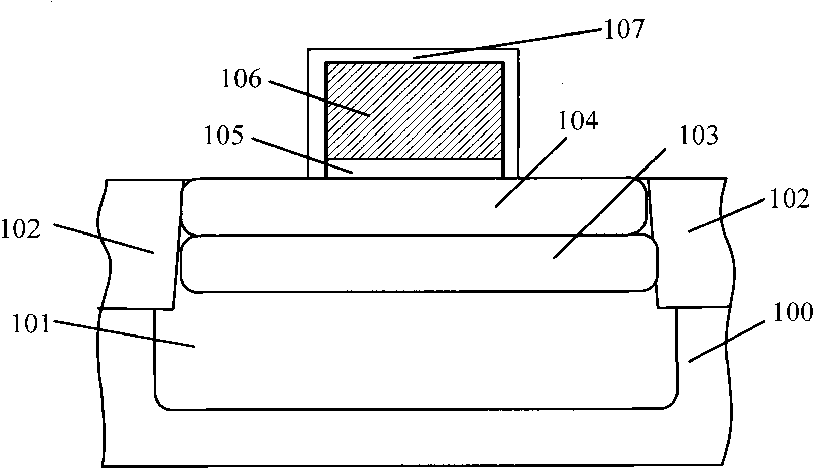
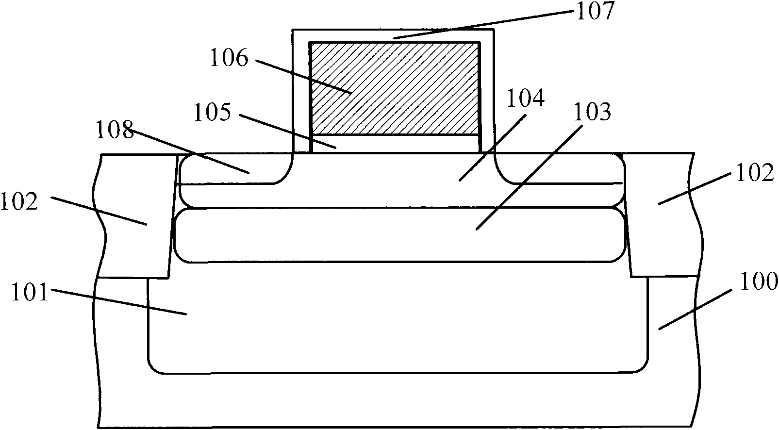
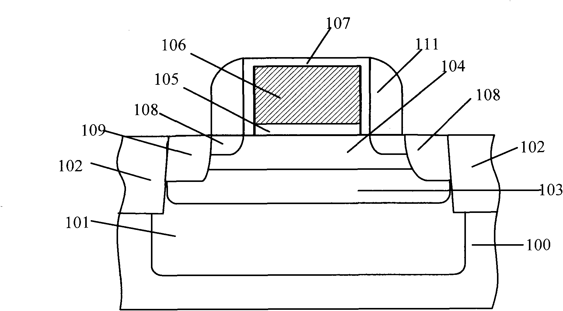
[0040] The inventors found that, in order to reduce the size of the device and suppress the short channel effect of the device, the prior art utilizes an ultra-shallow junction process to fabricate the source / drain regions of the MOS transistor. Since the depth of the source / drain region is reduced, the depth of the threshold voltage injection region in the prior art should also be correspondingly reduced. However, the depth of the threshold voltage implantation region is reduced, so that the activation rate of the dosage of the threshold voltage implantation is reduced, and the effect of the threshold voltage implantation on the threshold voltage adjustment of the transistor becomes worse. In order to obtain the same adjustment effect, the prior art increases the dose of threshold voltage implantation, but because the element of threshold voltage implantation is usually boron (for NMOS transistors) or phosphorus (for PMOS transistors), large doses of boron and phosphorus are p...


PUM


Abstract

The invention provides an MOS transistor and a manufacturing method thereof. The manufacturing method comprises the following steps: providing a semiconductor substrate; carrying out non-crystallization ion implantation on the semiconductor substrate, and forming a non-crystallization region in the semiconductor substrate; carrying out threshold voltage injection on the semiconductor substrate, and forming a threshold voltage injection region on the non-crystallization region; forming a gate structure at a semiconductor substrate surface above the threshold voltage injection region; forming a source/drain region in the semiconductor substrate at two sides of the gate structure. According to the MOS transistor and the manufacturing method in the invention, junction capacitance of the MOS transistor is reduced, a response speed of the MOS transistor is raised, and leakage current of the MOS transistor is reduced.

Description

technical field [0001] The invention relates to the field of semiconductors, in particular to a MOS transistor and a manufacturing method thereof. Background technique [0002] Metal-oxide-semiconductor (MOS) transistors are the most basic devices in semiconductor manufacturing. They are widely used in various integrated circuits. According to the different conductivity types of the main carriers, they are divided into NMOS and PMOS transistors. [0003] Taking NMOS transistors as an example, please refer to Figure 1 to Figure 3 , is a schematic cross-sectional structure diagram of a conventional NMOS transistor manufacturing method. [0004] Please refer to figure 1 , providing a semiconductor substrate 100 with isolation structures 102 formed in the semiconductor substrate 100, the semiconductor substrate between adjacent isolation structures 102 is an active region, and a doped well 101 is formed in the active region , the conductivity type of the doped well 101 is P ...

Claims


Application Information

Patent Timeline
Patent Type & Authority Applications(China)
IPC IPC(8): H01L21/336H01L21/265H01L29/78H01L29/06
Inventor 赵猛
Owner SEMICON MFG INT (SHANGHAI) CORP
Why Eureka
Try Eureka