Semiconductor structure and forming method thereof

A semiconductor and overall technology, applied in the direction of semiconductor devices, semiconductor/solid-state device manufacturing, semiconductor/solid-state device components, etc., can solve problems such as interface fracture, achieve the effect of reducing surface stress and improving adhesion

Active Publication Date: 2012-05-23
SEMICON MFG INT (SHANGHAI) CORP +1
View PDF5 Cites 14 Cited by
  • Summary
  • Abstract
  • Description
  • Claims
  • Application Information

AI Technical Summary

Problems solved by technology

[0008] The problem solved by the present invention is to provide a semiconductor structure and its formation method to solve the problem of interface fracture between the NDC material and the adjacent dielectric layer in the existing composite diffusion barrier layer

Method used


Image

  • Semiconductor structure and forming method thereof
  • Semiconductor structure and forming method thereof
  • Semiconductor structure and forming method thereof

Examples


Embodiment Construction

[0018] In order to make the above objects, features and advantages of the present invention more comprehensible, specific implementations of the present invention will be described in detail below in conjunction with the accompanying drawings.

[0019] In the following description, many specific details are set forth in order to fully understand the present invention, but the present invention can also be implemented in other ways than those described here, so the present invention is not limited by the specific embodiments disclosed below.

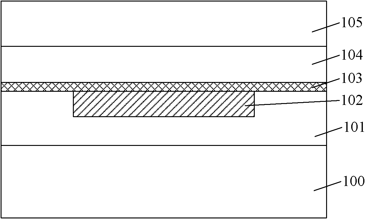
[0020] As described in the background technology section, since there is a large stress difference between the metal adhesion layer made of NDC and the intermetallic dielectric layer made of SiOCH, the adhesion is poor, so it is prone to fracture. The surface of the material is treated with plasma bombardment to reduce its surface stress and improve the adhesion with SiOCH material to solve the above defects.

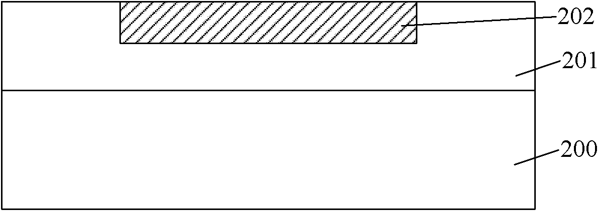
[0021] refer to figure 2 ...


PUM


Abstract

The invention provides a semiconductor structure and a forming method thereof. The forming method comprises the following steps of: providing a semiconductor substrate; forming a first dielectric layer on the surface of the semiconductor substrate; forming a metal blocking layer on the surface of the first dielectric layer; forming a metal adhesion layer made of NDC (Naphthalene Dicarboxylate) materials on the surface of a metal diffusion layer; sequentially carrying out Ar ion and oxygen ion bombardment on the surface of the metal adhesion layer; and forming a second dielectric layer on the surface of the metal adhesion layer. A compact oxide film can be formed on the surface made of NDC materials, so that the surface stress is reduced, the adhesivity between the NDC materials and the adjacent dielectric layers is improved, and meanwhile, the electrical performance of the device cannot be influenced.

Description

technical field [0001] The present invention relates to the field of semiconductor technology, and more specifically, the present invention relates to a semiconductor structure with a metal interconnection structure and a method for forming the same. Background technique [0002] In integrated circuit technology, silicon dioxide, which has thermal stability and moisture resistance, has always been the main insulating material used between metal interconnection lines, and metal aluminum is the main material for circuit interconnection wires in chips. However, relative to the miniaturization of components and the increase in integration, the number of conductor connections in the circuit continues to increase, making the parasitic effects of resistance (R) and capacitance (C) in the conductor connection structure, causing serious problems. Transmission delay (RC Delay) and crosstalk (Cross Talk) become the main factors that limit the signal transmission speed in the circuit in...

Claims


Application Information

Patent Timeline
Patent Type & Authority Applications(China)
IPC IPC(8): H01L21/768H01L23/522H01L23/532
Inventor 周鸣
Owner SEMICON MFG INT (SHANGHAI) CORP
Why Eureka
Try Eureka