Solar cell and preparation method thereof
A technology of solar cells and sheet resistance, applied in circuits, photovoltaic power generation, electrical components, etc., can solve the problems of inability to accurately control the concentration of doping ions, low conversion efficiency of solar cells, complicated process steps, etc., and improve the conversion efficiency of solar energy. , The effect of improving the utilization rate and improving the conversion efficiency
- Summary
- Abstract
- Description
- Claims
- Application Information
AI Technical Summary
Problems solved by technology
Method used
Image

Examples
preparation example Construction
[0046] refer to Figure 1-Figure 8 , introduce in detail the preparation method of the solar cell of the present invention, it comprises the following steps:
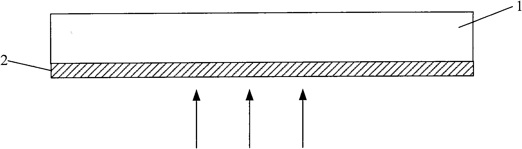
[0047] refer to figure 1 , step S 1 , form the P+ type doped layer 2 on the wafer back side of the P type substrate 1, and those skilled in the art can select a suitable process for forming the doped layer according to actual needs, such as accelerating P type ions and forming the P+ type by ion implantation. In the doped layer 2, P-type ions are accelerated to 500eV-50keV, and the sheet resistance of the formed P+-type doped layer is 20-60Ω / □. Those skilled in the art can select appropriate dopant ions and the concentration and energy of the dopant ions according to actual needs to obtain ideal sheet resistance. For example, P-type ions are accelerated to 1keV-40keV, preferably, P-type ions are accelerated to 5keV-30keV; the sheet resistance of the formed P+ type doped layer is 25-55Ω / □, preferably, the formed P+ T...
Embodiment 1
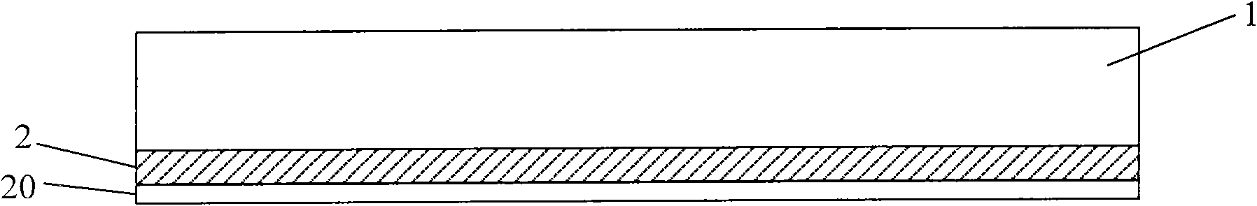
[0065] refer to figure 1 , step S 1 , form a P+ type doped layer 2 on the back of the wafer of the P type substrate 1. In this embodiment, P type ions are accelerated and the P+ type doped layer 2 is formed by ion implantation, wherein boron ions are accelerated to 500eV, and the formed The sheet resistance of the P+ type doped layer is 20Ω / □. Since the P+ type doped layer is formed by ion implantation, an annealing step is required, figure 1 The direction of ion implantation shown by the middle arrow is only for easy understanding and should not be construed as a limitation of the present invention. After the ion implantation is completed, annealing is performed to activate the doped impurities.
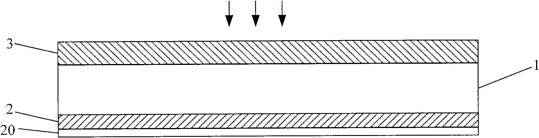
[0066] refer to Figure 2-3 , step S 2 , forming an N-type doped layer 3 on the wafer surface of the P-type substrate 1, wherein the N-type doped layer 3 is formed by thermal diffusion, and the sheet resistance of the N-type doped layer 3 is 60Ω / □. In this embodiment select PO...
Embodiment 2
[0072] refer to figure 1 , step S 1 , form a P+ type doped layer 2 on the back of the wafer of the P type substrate 1. In this embodiment, P type ions are accelerated and the P+ type doped layer 2 is formed by ion implantation, wherein boron ions are accelerated to 50keV, and the formed The sheet resistance of the P+ type doped layer is 60Ω / □. Since the P+ type doped layer is formed by ion implantation, an annealing step is required, figure 1 The direction of ion implantation shown by the middle arrow is only for easy understanding and should not be construed as a limitation of the present invention. After the ion implantation is completed, annealing is performed to activate the doped impurities.
[0073] refer to Figure 2-3 , step S 2 , forming an N-type doped layer 3 on the wafer surface of the P-type substrate 1, wherein the N-type doped layer 3 is formed by thermal diffusion, and the sheet resistance of the N-type doped layer 3 is 120Ω / □, in this embodiment select...
PUM
| Property | Measurement | Unit |
|---|---|---|
| Sheet resistance | aaaaa | aaaaa |
| Sheet resistance | aaaaa | aaaaa |
| Resistance | aaaaa | aaaaa |
Abstract
Description
Claims
Application Information
 - Generate Ideas
- Intellectual Property
- Life Sciences
- Materials
- Tech Scout
- Unparalleled Data Quality
- Higher Quality Content
- 60% Fewer Hallucinations
Browse by: Latest US Patents, China's latest patents, Technical Efficacy Thesaurus, Application Domain, Technology Topic, Popular Technical Reports.
© 2025 PatSnap. All rights reserved.Legal|Privacy policy|Modern Slavery Act Transparency Statement|Sitemap|About US| Contact US: help@patsnap.com