N-i-n type electro-optic modulator

An electro-optic modulator, n-i-n technology, applied in the direction of instruments, optics, nonlinear optics, etc., can solve the problems of inability to form current blocking, difficult electric field electro-optic modulation, and reduce modulation efficiency, so as to improve the secondary electro-optic effect and reduce leakage current , the effect of improving the modulation characteristics

Active Publication Date: 2014-07-02
TSINGHUA UNIV
View PDF4 Cites 0 Cited by
  • Summary
  • Abstract
  • Description
  • Claims
  • Application Information

AI Technical Summary

Problems solved by technology

But this structure has a defect: the InP layer has to divide a large part of the voltage, which reduces the modulation efficiency, making it difficult to further reduce the half-wave voltage.
However, there is no reverse-biased PN junction in the general n-i-n structure, and current blocking cannot be formed. Electronic current is formed after voltage is applied, and it is difficult to form an effective electric field for electro-optic modulation.
There is no public literature on n-i-n electro-optic modulators at home and abroad

Method used


Image

  • N-i-n type electro-optic modulator
  • N-i-n type electro-optic modulator
  • N-i-n type electro-optic modulator

Examples


Embodiment 1

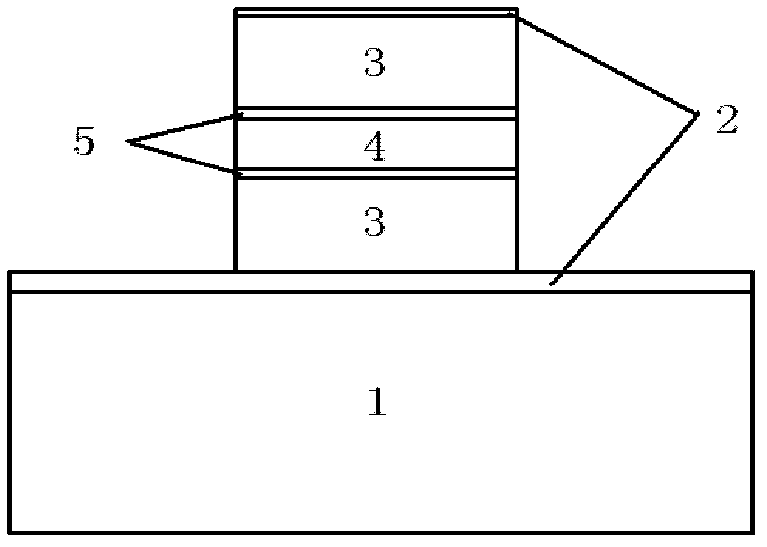
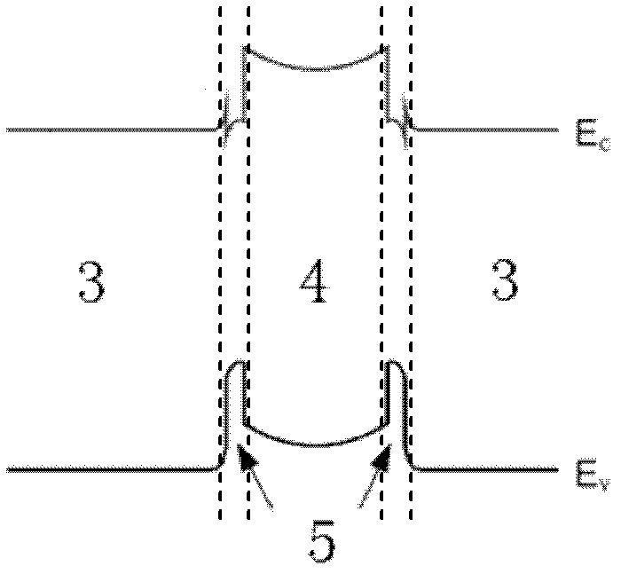
[0028] Such as Figure 3a Shown is the structure of the InP-InAlAs-InP semiconductor electro-optic modulator based on InP, and its energy band structure diagram is as follows Figure 3b shown. Wherein, the confinement layer is an N-type doped InP confinement layer 13 with a doping concentration of 10 17 order of magnitude. The ohmic contact layer is made of N-type doped InGaAs material, which is the N-type doped InGaAs ohmic contact layer 10 . The active layer (also known as the active region) uses InP lattice-matched InAlAs (E g =1.45eV) bulk material is the InAlAs active layer 11, the waveguide width is 2um, and the thickness of the InAlAs active layer 11 is 390nm. On both sides of the InAlAs active layer 11, InGaAsP (E g =0.95eV) The purpose of the waveguide layer 12 is to confine the light field more effectively. In order to reduce the electrical loss of the microwave signal, the substrate is a semi-insulating InP substrate 9, and the waveguide adopts a high ridge st...

Embodiment 2

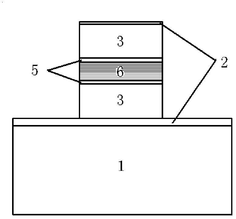
[0036] Such as Figure 4a As shown, the active layer can use 20 cycles of InGaAsP (E g =0.95eV) / InAlAs(E g =1.45eV) n-i-n structure of quantum wells, which is N-type doped InGaAsP / InAlAs (' / ' represents quantum wells, the left side of ' / ' is a well, and the right side is a barrier) multi-quantum well active layer 14, the total of the active layer The thickness is 390nm. In order to effectively confine the optical field, a 50nm InGaAsP (E g =0.95eV) waveguide layer 12 . Since InGaAsP(E g =0.95eV) / InAlAs(E g =1.45eV) The potential barrier formed by multiple quantum wells not only has the effect of blocking leakage current, but also because the energy band structure of multiple quantum wells can form a certain reflection on electrons, the energy band structure in the case of quantum wells can be more effectively Block leakage current. Through calculation, it can be concluded that the leakage current of the quantum well structure is an order of magnitude smaller than that o...


PUM

PropertyMeasurementUnit
lengthaaaaaaaaaa

Abstract

The invention relates to the field of photoelectronic devices in optical communication, and discloses an n-i-n type electro-optic modulator, which comprises a substrate, a lower ohmic contact layer, a lower limit layer, a lower wave guide layer, an active layer, an upper wave guide layer, an upper limit layer and an upper ohmic contact layer from bottom to top. The upper limit layer and the lower limit layer are in N type doped structures. The active layer has a forbidden bandwidth Eg1 and refractive index n1. The upper wave guide layer and the lower wave guide layer have forbidden bandwidth Eg2 and refractive indexes n2, the upper limit layer and the lower limit layer have forbidden bandwidth Eg3 and refractive indexes n3, the forbidden bandwidth is in the relation Eg1>Eg3>Eg2, and the refractive indexes are in the relation n2>n1>n3. The modulation character of the electro-optic modulator can be improved.

Description

technical field [0001] The invention relates to the field of optoelectronic devices in optical communication, in particular to an n-i-n type electro-optic modulator. Background technique [0002] Electro-optic modulators play a vital role in the field of fiber optic communications, especially in spectrally efficient fiber optic networks utilizing advanced modulation formats. The driving voltage is one of the important parameters of the electro-optic modulator, and a lower driving voltage helps to improve system characteristics and reduce power loss. with LiNbO 3 Compared with basic electro-optic modulators, III-V electro-optic modulators have the advantages of compact structure, low half-wave voltage, and easy integration. They can play an increasingly important role in the field of optical communication in the future. [0003] The traditional III-V semiconductor electro-optic modulator adopts a reverse biased p-i-n structure, which has the advantage of high voltage loadin...

Claims


Application Information

Patent Timeline
Patent Type & Authority Patents(China)
IPC IPC(8): G02F1/017
Inventor 孙长征郭丽丽熊兵罗毅赵湘楠
Owner TSINGHUA UNIV
Why Eureka
Try Eureka