

Electro-optic modulator and manufacturing method thereof
An electro-optical modulator, metal electrode technology, applied in instruments, optics, nonlinear optics, etc., can solve problems such as microwave loss, achieve high-efficiency electric field loading, solve microwave loss, and improve modulation characteristics.
- Summary
- Abstract
- Description
- Claims
- Application Information
AI Technical Summary
Problems solved by technology
Method used
Image

Examples
Embodiment 1
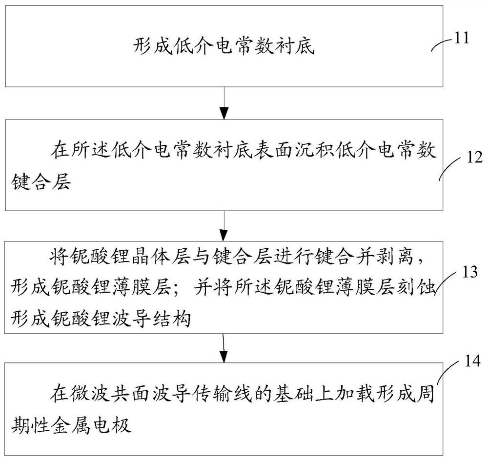
[0020] figure 1 It is a schematic flow chart of a manufacturing method of an electro-optic modulator according to an embodiment of the present invention, the method comprising:
[0021] Step 11, forming a low dielectric constant substrate;
[0022] The low dielectric constant substrate is quartz crystal with a thickness ranging from 100um to 500um.
[0023] Step 12, depositing a low dielectric constant bonding layer on the surface of the low dielectric constant substrate;
[0024] The low dielectric constant bonding layer is a silicon dioxide layer or a benzocyclobutene (BCB) layer with a thickness ranging from 2um to 10um.
[0025] Step 13, bonding and peeling off the lithium niobate crystal layer and the bonding layer to form a lithium niobate thin film layer; and etching the lithium niobate thin film layer to form a lithium niobate waveguide structure;
[0026] Wherein, the thickness of the lithium niobate thin film layer ranges from 400nm to 800nm. When etching the lit...
Embodiment 2
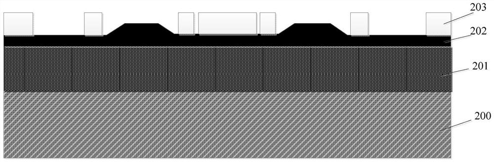
[0039] Figure 4 It is a schematic flow chart of the manufacturing method of the second electro-optic modulator of the present invention, combined below Figure 4a to Figure 4e The specific structural schematic diagram in the method preparation is described in detail. The method includes:
[0040] Step 41, such as Figure 4a As shown, a low dielectric constant substrate 200 is formed;
[0041] The low dielectric constant substrate is quartz crystal with a thickness ranging from 100um to 500um.
[0042] Step 42, such as Figure 4b As shown, a low dielectric constant bonding layer 201 is deposited on the surface of the low dielectric constant substrate;
[0043] The low dielectric constant bonding layer is a silicon dioxide layer or a benzocyclobutene (BCB) layer with a thickness ranging from 2um to 10um.
[0044] Step 43, such as Figure 4cAs shown, the lithium niobate crystal layer and the bonding layer are bonded and peeled off to form a lithium niobate thin film layer...
Embodiment 3
[0052] Figure 5 It is a schematic flow chart of a method for manufacturing an electro-optic modulator according to Embodiment 3 of the present invention, and the method includes:
[0053] Step 51, forming a low dielectric constant substrate 200;
[0054] The low dielectric constant substrate is quartz crystal with a thickness ranging from 100um to 500um.
[0055] Step 52, depositing a low dielectric constant bonding layer 201 on the surface of the low dielectric constant substrate;
[0056] The low dielectric constant bonding layer is a silicon dioxide layer or a benzocyclobutene (BCB) layer with a thickness ranging from 2um to 10um.
[0057] Step 53, removing the low dielectric constant bonding layer below the effective modulation region of the lithium niobate waveguide structure to form a bonding layer 201';
[0058] When the bonding layer is a silicon dioxide layer, dry etching or wet etching is used to remove the low dielectric constant bonding layer below the effectiv...
PUM
| Property | Measurement | Unit |
|---|---|---|
| thickness | aaaaa | aaaaa |
Abstract
Description
Claims
Application Information