Process for manufacturing printed circuit boards having high-frequency and low-frequency mixed board structures

A technology of printed circuit board and manufacturing process, which is applied in the direction of printed circuit manufacturing, printed circuit, printed circuit components, etc., can solve the problems of delamination and explosion, achieve the goal of reducing volume, saving cost, and improving product assembly density Effect

Inactive Publication Date: 2012-06-27
SHENZHEN SUNTAK MULTILAYER PCB
View PDF4 Cites 29 Cited by
  • Summary
  • Abstract
  • Description
  • Claims
  • Application Information

AI Technical Summary

Problems solved by technology

[0003] The purpose of the present invention is to provide a method that can effectively control the warping defect of the high-frequ...

Method used


Image

  • Process for manufacturing printed circuit boards having high-frequency and low-frequency mixed board structures
  • Process for manufacturing printed circuit boards having high-frequency and low-frequency mixed board structures
  • Process for manufacturing printed circuit boards having high-frequency and low-frequency mixed board structures

Examples


Embodiment Construction

[0021] The present invention will be described in further detail below in conjunction with specific embodiments and accompanying drawings.

[0022] 1) Cutting material:

[0023] l When cutting the material, it is necessary to measure the thickness of the cutting substrate within the tolerance range to ensure that the cutting plate can meet the thickness requirements of the laminated plate;

[0024] l Cutting size: 605*300mm; material: IT158 and RF-35;

[0025] 2) Inner graphics:

[0026] l Make the inner layer graphics of high-frequency panels and low-frequency panels;
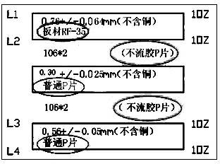
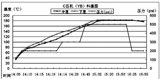
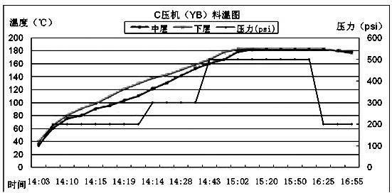
[0027] 3) Pressing

[0028] l Browning: browning of light board and core board, browning speed: 3.0~3.2m / min;

[0029] l Pressing: A. The hot pressing parameters are shown in Table 1: use the following parameters; kraft paper: 20 sheets (new) for each top and bottom;

[0030] B. When typesetting, pay attention to cleaning the PP powder on the copper surface of the step plate;

[0031] C. The number of la...


PUM


Abstract

The invention discloses a process for manufacturing printed circuit boards having high-frequency and low-frequency mixed board structures, which includes steps of A) cutting high-frequency boards and low-frequency boards, manufacturing inner patterns, performing brownification, pressing, removing liquid adhesives and drilling holes; B) removing adhesives by plasmas, plating copper outside the high-frequency and low-frequency pressed board with drilled holes and electroplating the integral pressed board; C) forming outer patterns; D) printing solder mask and texts after solder mask of plug holes in a screen manner; E) printing characters after plating the integral board with nickel and gold and forming a circuit board in a screen manner; and F) testing and detecting electric performance and appearance of a finished board and manufacturing the finished product. By the design of the high-frequency and low-frequency mixed press structure, a necessary layer can be made of high-frequency boards with PTFE (poly tetra fluoro ethylene) structures so as to guarantee high speed and undistorted transmission of signals and the requirement of impedance matching, and other signal layers can be made of common boards with epoxy resin substrates on the condition of meeting the requirements of the integral performance, and cost is saved for clients by optimized combination.

Description

technical field [0001] The invention belongs to the field of printed circuit boards, and in particular relates to a high-frequency-low-frequency mixed plate structure printed circuit board anti-warping manufacturing process. Background technique [0002] With the rapid development of communication and electronics industries and the subsequent development trend of high-frequency and high-speed transmission performance requirements for information data, the global PCB scale and technology are constantly updated. Driven by this trend, a high-frequency mixed-voltage ladder has emerged Printed circuit board design. However, when high frequency and low frequency are mixed, it often leads to delamination, cracking, and warping, which seriously affects the performance of the product. Contents of the invention [0003] The object of the present invention is to provide a method that can effectively control the warping defect of the high-frequency-low-frequency mixed plate structure...

Claims


Application Information

Patent Timeline
IPC IPC(8): H05K3/00
CPCH05K1/024H05K3/00B32B37/10H05K1/036
Inventor 宋建远姜雪飞朱拓谢萍萍
Owner SHENZHEN SUNTAK MULTILAYER PCB
Why Eureka
Try Eureka