
Silicon carbide crystal annealing process

An annealing process, silicon carbide technology, applied in crystal growth, single crystal growth, single crystal growth, etc., can solve problems such as crystal cracking

Active Publication Date: 2012-07-04
BEIJING TIANKE HEDA SEMICON CO LTD
View PDF9 Cites 30 Cited by
  • Summary
  • Abstract
  • Description
  • Claims
  • Application Information

AI Technical Summary

Problems solved by technology

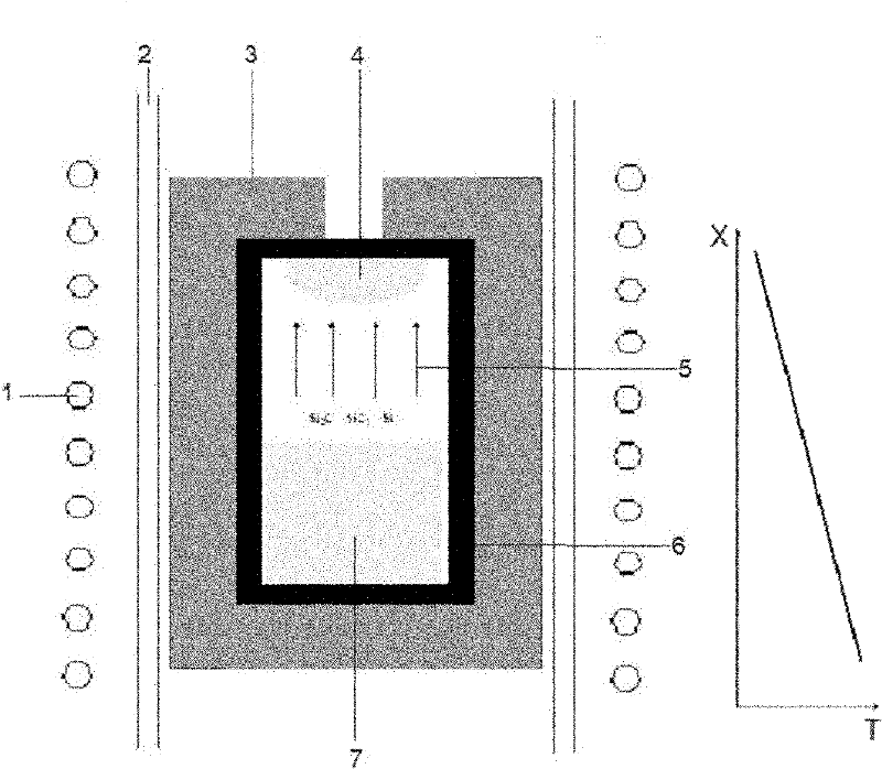
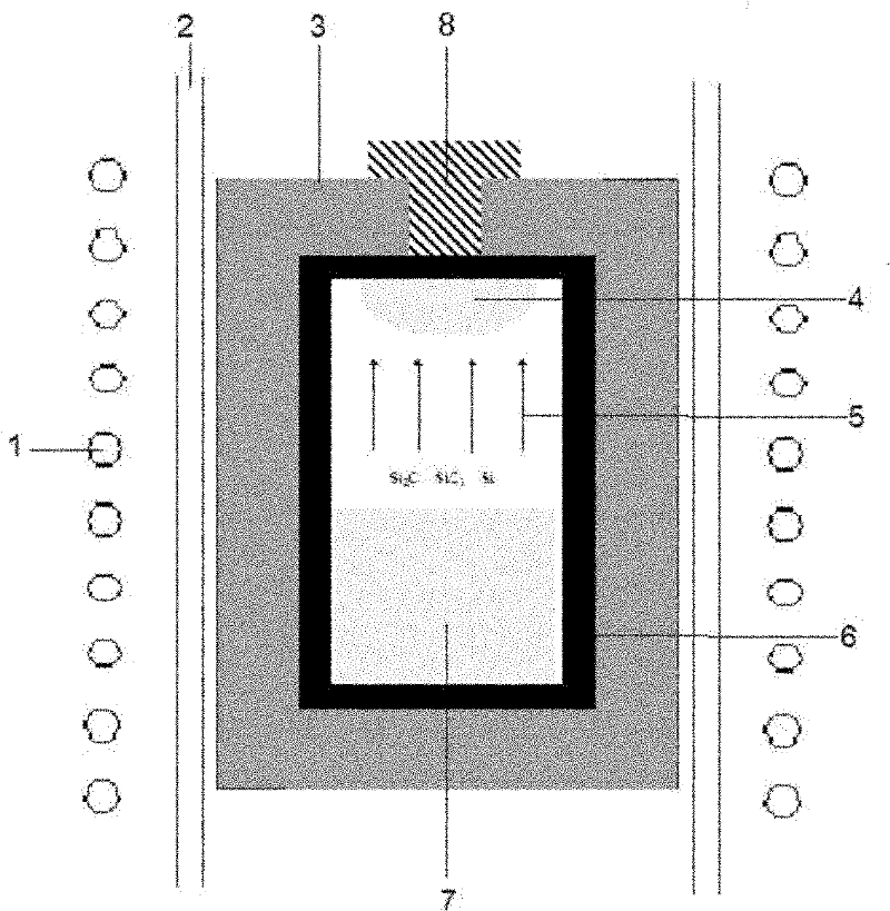
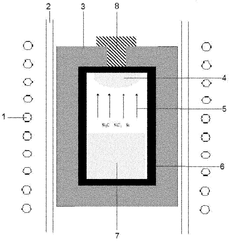
[0006] Aiming at the serious problem of cracking of the crystal due to mechanical action during the process of taking silicon carbide crystal from the crucible cover, secondary annealing and subsequent processing of the crystal, especially when the crystal is ground and rolled, the present invention mainly optimizes the principle In-situ annealing process reduces the stress between the silicon carbide crystal and the crucible cover and inside the silicon carbide crystal, thereby eliminating the problem of crystal cracking caused by taking the crystal from the crucible cover, secondary annealing and subsequent processing of the crystal, and improving the yield of silicon carbide crystal

Method used


Image

  • Silicon carbide crystal annealing process
  • Silicon carbide crystal annealing process
  • Silicon carbide crystal annealing process

Examples


Embodiment 1

[0028] The designed insulation layer ensures that the placement of the insulation layer at the annealing temperature can reduce the crystal temperature gradient from about 20°C / cm to below 5°C / cm. After the growth of the 2-inch 6H semi-insulating silicon carbide crystal is completed, the insulation layer is placed in the heat dissipation hole with a mechanical device. The whole process takes 2 hours and the temperature is raised. It also takes 2 hours to raise the temperature to 2300 ° C. After placing The insulation layer and the increase of the crystal temperature increase the argon pressure in the growth chamber at the same time, and the pressure is raised from 2 kPa to 20 thousand Pa in 2 hours. When the temperature is constant for 20 hours, it takes 22 hours to cool down from 2300°C to 100°C at a speed of 100°C / h, and then turn off the power directly.

Embodiment 2

[0030]The designed insulation layer ensures that the placement of the insulation layer at the annealing temperature can reduce the crystal temperature gradient from about 25°C / cm to below 5°C / cm. After the growth of the 3-inch 4H conductive silicon carbide crystal is completed, the thermal insulation layer is placed in the heat dissipation hole with a mechanical device. The whole process takes 3 hours, and the temperature is raised. It also takes 3 hours to raise the temperature to 2300°C. layer and increase the crystal temperature while increasing the argon pressure in the growth chamber, and the pressure was raised from 2 kPa to 30,000 Pa in 3 hours. When the temperature is constant for 30 hours, it takes 22 hours to cool down from 2300°C to 100°C at a speed of 100°C / h, and then turn off the power directly.

Embodiment 3

[0032] The designed insulation layer ensures that the placement of the insulation layer at the annealing temperature can reduce the crystal temperature gradient from about 30°C / cm to below 5°C / cm. After the growth of the 4-inch 4H conductive silicon carbide crystal is completed, the insulation layer is placed in the heat dissipation hole with a mechanical device. The whole process takes 4 hours, and the temperature is raised. It also takes 4 hours to raise the temperature to 2400°C. layer and increase the crystal temperature while increasing the argon pressure in the growth chamber, and the pressure was increased from 2 kPa to 40,000 Pa in 4 hours. When the temperature is constant for 30 hours, it takes 23 hours to cool down from 2400°C to 100°C at a speed of 100°C / h, and then turn off the power directly.


PUM

PropertyMeasurementUnit
sizeaaaaaaaaaa

Abstract

The invention is mainly applied to the field of treatment after silicon carbide crystal growth completion and particularly relates to a silicon carbide crystal annealing process which is specifically characterized by reducing the temperature gradient (the temperature gradient of the crystals is 1-10 DEG C / cm), spending 1-5 hours in raising the temperature to the annealing temperature under the inert gases with pressure of above 0.01-0.08MPa and then spending 10-50 hours in reducing the temperature after keeping the constant temperature for 10-40 hours, wherein the annealing temperature is 2300-2500 DEG C. By adopting the annealing process, the stress between the crystals and a crucible cover and the stress inside the silicon carbide crystals are reduced, thus reducing the damage rate of the silicon carbide crystals in the follow-up processing course and improving the yield of the silicon carbide crystals.

Description

technical field [0001] The invention is mainly used in the field of after-treatment of silicon carbide crystal growth, specifically, by improving the annealing process, reducing the stress between the crystal and the crucible cover and the internal stress of the crystal to reduce the crystal damage rate in the subsequent processing process, thereby increasing the crystal yield . Background technique [0002] With the rapid development of information technology today, the innovation of semiconductor technology plays an increasingly important role. Wide bandgap semiconductor materials represented by silicon carbide and gallium nitride are the third generation of wide bandgap semiconductors after silicon and gallium arsenide. Compared with traditional semiconductor materials represented by silicon and gallium arsenide, silicon carbide has great advantages in terms of operating temperature, radiation resistance, breakdown voltage and other properties. As the most mature wide b...

Claims


Application Information

Patent Timeline
Patent Type & Authority Applications(China)
IPC IPC(8): C30B33/02C30B29/36
CPCC30B23/06C30B33/02C30B29/36C30B23/002
Inventor 王波陈小龙李龙远刘春俊彭同华王刚
Owner BEIJING TIANKE HEDA SEMICON CO LTD
Learn More