Novel silicon carbide MOSFET (Metal Oxide Semiconductor Field Effect Transistor)

A new type of silicon carbide technology, applied in electrical components, circuits, semiconductor devices, etc., can solve problems such as gate insulating layer breakdown, reduce the probability of breakdown, improve the overall withstand voltage, and prevent breakdown.

Inactive Publication Date: 2012-07-04
ZHEJIANG UNIV
View PDF6 Cites 2 Cited by
  • Summary
  • Abstract
  • Description
  • Claims
  • Application Information

AI Technical Summary

Problems solved by technology

[0004] Aiming at the breakdown problem of the gate insulation layer in current high-voltage silicon carbide MOSFET design, the present invention proposes a novel silicon carbide MOSFET

Method used


Image

  • Novel silicon carbide MOSFET (Metal Oxide Semiconductor Field Effect Transistor)
  • Novel silicon carbide MOSFET (Metal Oxide Semiconductor Field Effect Transistor)

Examples


Embodiment

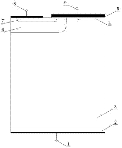
[0013] New silicon carbide MOSFETs such as figure 1 As shown, it includes a drain 1 arranged at the lower end, a source 8 and a gate 9 arranged at the upper end, a buffer zone 2 and a drift region 3 are sequentially connected above the drain 1, a source region 7 is arranged below the source 8, and a gate 9 is arranged below the source 8. A gate insulating layer 5 is arranged under the electrode 9 , and a P doped region 4 is arranged under the gate insulating layer 5 , and the P doped region 4 is connected to the upper right part of the drift region 3 .

[0014] A P well region 6 is provided below the source region 7 , and the P well region 6 is connected to the upper left part of the drift region 3 .


PUM


Abstract

The invention relates to a semiconductor device, and in particular discloses a novel silicon carbide MOSFET (Metal Oxide Semiconductor Field Effect Transistor) which is applied to occasions of electrical equipment such as an alternating current motor, a frequency converter, a switch power supply, traction transmission equipment and the like under high-voltage conditions. The novel silicon carbide MOSFET comprises a drain electrode (1) which is arranged at a lower end as well as a source electrode (8) and a gate electrode (9) which are arranged at an upper end, wherein a buffer region (2) and a drift region (3) are sequentially connected above the drain electrode (1), a source region (7) is arranged below the source electrode (8), a gate insulation layer (5) is arranged below the gate electrode (9), a P-type well region (6) is arranged below the source region (7), and a P-type doping region (4) is arranged below the gate insulation layer (5). According to the invention, on the basis of a common MOSFET structure, the doping region with low concentration is additionally arranged on the surface of a substrate below the gate electrode so that an electric field in the gate insulation layer is weakened when the high voltage is applied to the device, thereby lowering the breakdown probability of the insulation layer and improving the integral withstand voltage of the silicon carbide MOSFET.

Description

technical field [0001] The invention relates to a semiconductor device, in particular to a novel silicon carbide MOSFET device used in electrical equipment under high voltage conditions, such as AC motors, frequency converters, switching power supplies, traction drives and the like. Background technique [0002] The main structure of a metal oxide field effect transistor (MOSFET) includes an emitter region, a channel region, and a drift region. By applying an electric field perpendicular to the surface of the material, an inversion layer is formed on the surface close to the gate to form a conductive channel. Due to the principle of unipolar conduction, MOSFET devices have the advantage of high switching speed. [0003] However, during the design and application process of silicon carbide MOSFET devices with higher withstand voltage, the breakdown of the gate insulating material leads to early breakthrough of the device, which limits the design and application of higher with...

Claims


Application Information

Patent Timeline
Patent Type & Authority Applications(China)
IPC IPC(8): H01L29/78H01L29/06
Inventor 盛况郭清蔡超峰崔京京周伟成
Owner ZHEJIANG UNIV
Why Eureka
Try Eureka