Supercharge Your Innovation With Domain-Expert AI Agents!

Method of preparing 1550nm laser utilizing silicon-based InGaAsP as active area

A technology of lasers and active regions, applied in lasers, laser components, semiconductor lasers, etc., can solve the problem that the silicon-based light emission problem has not been solved well, affect the quality of the epitaxial layer, etc., to reduce defects, improve quality, The effect of improving injection efficiency

Active Publication Date: 2012-07-04
湖北航星光电科技股份有限公司
View PDF3 Cites 7 Cited by
  • Summary
  • Abstract
  • Description
  • Claims
  • Application Information

AI Technical Summary

Problems solved by technology

However, the problem of silicon-based luminescence has not been well resolved
These dislocations and antiphase domain boundaries will extend all the way to the surface of the epitaxial layer, seriously affecting the quality of the epitaxial layer

Method used


Image

  • Method of preparing 1550nm laser utilizing silicon-based InGaAsP as active area
  • Method of preparing 1550nm laser utilizing silicon-based InGaAsP as active area
  • Method of preparing 1550nm laser utilizing silicon-based InGaAsP as active area

Examples


Embodiment Construction

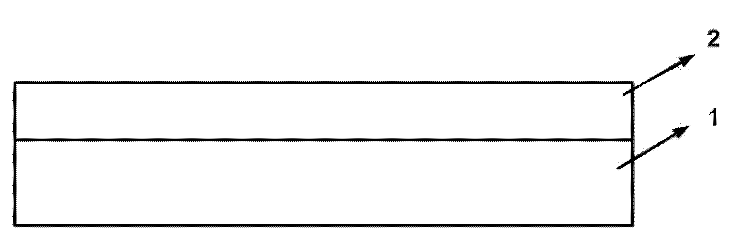
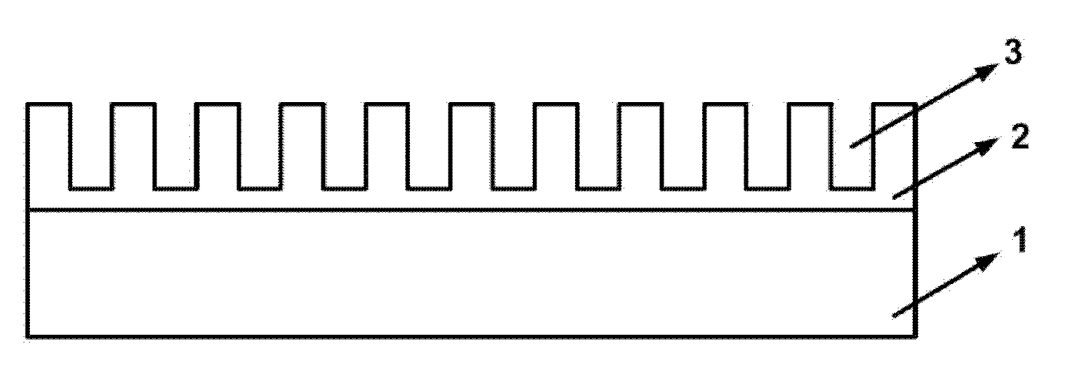
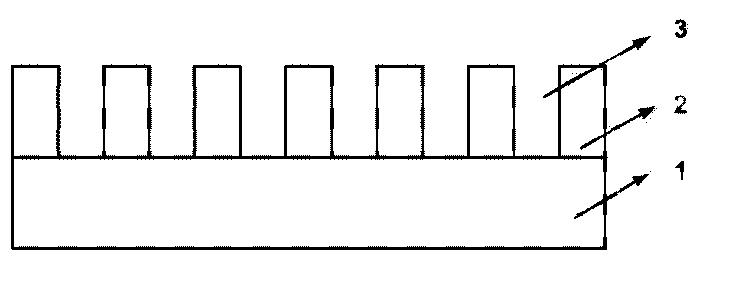
[0025] see Figure 1 to Figure 10 , the invention provides a method for preparing a silicon-based InGaAsP 1550nm laser with an active region, comprising the following steps:

[0026] Step 1: growing a silicon dioxide layer 2 on a silicon substrate 1, wherein the silicon substrate 1 is n-type high-resistance (001) silicon, the resistivity is greater than 2000 ohm cm, and the thickness of the silicon dioxide layer 2 is 500nm- 600nm.

[0027] Step 2: using holographic exposure and ICP methods to etch a groove 3 on the silicon dioxide layer 2 along the direction of the silicon substrate 1, the width of which is 200-300 nm, and the depth is the same as the thickness of the silicon dioxide layer 2 same, and more than ten nanometers of silicon dioxide is left at the bottom of the trench 3 to protect the silicon substrate 1 .

[0028] Step 3: Use piranha and SC respectively 2 , HF and deionized water cleaning, remove the remaining silicon dioxide layer 2 at the bottom of the trenc...


PUM


Abstract

The invention claims a method of preparing a 1550nm laser utilizing silicon-based InGaAsP as an active area. The method comprises the following steps: growing a silica layer on a silicon substrate; etching a groove along the silicon substrate (110) on the silica layer; cleaning; sequentially growing a first buffer layer and a second buffer layer in the groove; then growing a third buffer layer onthe second buffer layer and the silica layer, and then growing a top layer on the third buffer layer; polishing the top layer, and then cleaning, wherein the roughness of the polished top layer is less than 1nm; sequentially extending a fourth buffer layer, an etching stop layer and a laser structure on the top layer; etching the laser structure to form a deep ridge, and etching a shallow ridge on the deep ridge; growing silica insulating layers on the surfaces of the deep ridge and the shallow ridge and the etching stop layer; forming a window on the shallow ridge, removing the silica insulating layer on the etching stop layer; sputtering a Ti-platinum P electrode on the window of the shallow ridge; and evaporating a Ge nickel gold N electrode on the etching stop layer; and annealing.

Description

technical field [0001] The invention relates to the technical field of semiconductors, in particular to a method for preparing a 1550nm laser with silicon-based InGaAsP as the active region. Background technique [0002] For the development of Optoelectronic Integrated Circuit (OEIC), the biggest problem is the lack of silicon-based light source. As the basis of microelectronic technology, silicon material is the most widely studied semiconductor material; the maturity of silicon processing technology is much higher than that of III-V compound semiconductor materials. However, the problem of silicon-based luminescence has not been well resolved. Considering the mature development of GaAs and InP lasers and their incompatibility with standard circuit technology, the preparation of silicon-based III-V compound semiconductor lasers is a feasible solution to the problem of silicon-based optical interconnection. As the minimum attenuation wavelength of optical fiber communicati...

Claims


Application Information

Patent Timeline
Patent Type & Authority Applications(China)
IPC IPC(8): H01S5/323
Inventor 周旭亮于红艳王伟潘教青王圩
Owner 湖北航星光电科技股份有限公司
Features
  • R&D
  • Intellectual Property
  • Life Sciences
  • Materials
  • Tech Scout
  • Unparalleled Data Quality
  • Higher Quality Content
  • 60% Fewer Hallucinations
Learn More