Manufacture method of liquid crystal display array substrate

A liquid crystal display and array substrate technology, which is applied in the field of manufacturing liquid crystal display array substrates, can solve the problems of poor etching performance, increased hydrogen peroxide decomposition rate, and poor stability of etching solution, etc.

Active Publication Date: 2012-07-11
DONGWOO FINE CHEM CO LTD
View PDF5 Cites 6 Cited by
  • Summary
  • Abstract
  • Description
  • Claims
  • Application Information

AI Technical Summary

Problems solved by technology

However, since metal ions, especially copper ions, dissolve when etching the metal layer, the decomposition rate of hydrogen peroxide may increase, undesirably generating overheating, and significantly deteriorating the stability of the etching solution.
[0006] Furthermore, in the case of metallic multilayers, due to electrical effects and the difference between the rate at which the copper layer is etched with hydrogen peroxide and the rate at which the molybdenum alloy layer is etched with fluorine compounds (this difference is related to the dissolved metal ions proportional to the increase in the concentration of ), so the interface between two mutually bonded metal layers may be deformed, resulting in poor etch performance

Method used


Image

  • Manufacture method of liquid crystal display array substrate
  • Manufacture method of liquid crystal display array substrate
  • Manufacture method of liquid crystal display array substrate

Examples


example

[0043] Preparation of etching solution composition

[0044] The etching solution compositions of Examples 1 to 6 were prepared using the components shown in Table 1 below.

[0045] Table 1

[0046] (Unit: wt%)

[0047] h 2 o 2

NH 4 f

Aminotetrazole

HEDP

Phosphate

Deionized water

Example 1

5

0.3

0.2

3.0

0.2

margin

Example 2

10

0.2

0.5

4.0

0.5

margin

Example 3

15

0.1

0.8

5.0

0.8

margin

Example 4

18

0.08

1.0

7.0

1.0

margin

Example 5

22

0.05

1.5

9.0

1.5

margin

Example 6

25

0.03

3.0

10.0

3.0

margin

[0048] *HEDP: 1-Hydroxyethylidene-1,1-diphosphate

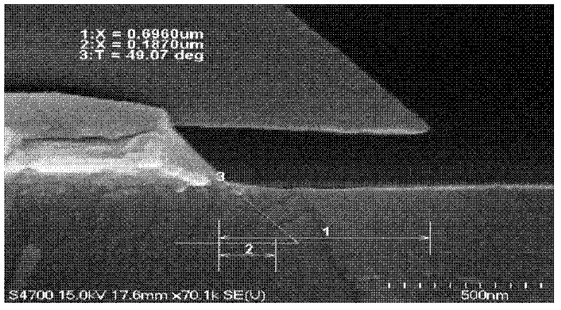
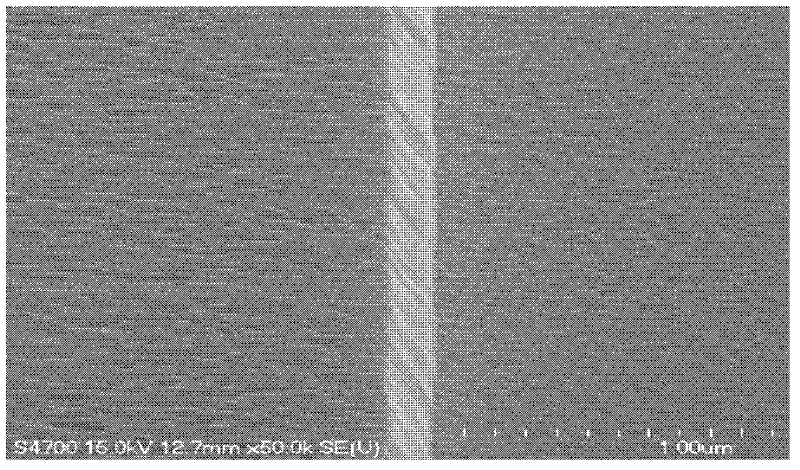
[0049] Etching of copper-based metal layer

[0050] A molybdenum-titanium (Mo-Ti) layer was deposited on a glass substrate (100mm×100mm), a co...


PUM


Abstract

The invention relates to a manufacture method of a liquid crystal display array substrate, comprising: forming a copper base metal layer on the substrate and forming an etched copper base metal layer by an etching solution to form a grid connection line; and forming a copper base metal layer on a semiconductor layer and forming an etched copper base metal layer by an etching solution to form a source electrode and a drain electrode, wherein based on the total weight of the above components, the etching solution comprises: A) hydrogen peroxide, B) fluorine compound, C) 0.1-5wt% of pyrryl compound; D) one or much compounds selected from phosphonic acid derivative or its salt, E) phosphate compound and F) water as residual.

Description

technical field [0001] The invention relates to a method for manufacturing an array substrate of a liquid crystal display, an etching solution composition for etching a copper-based metal layer, and a method for etching a copper-based metal layer by using the etching solution composition. Background technique [0002] A method of forming metal wiring on a substrate of a liquid crystal display generally includes forming a metal layer by sputtering, coating a photoresist, exposing and developing to form a photoresist on a selected area, and performing etching, in each of the above steps Before or after the cleaning process. performing an etching process so that the metal layer is left on the selected areas using the photoresist as a mask, and the etching process may include dry etching using plasma or the like or wet etching using the composition of the etching solution. etched. [0003] The focus of recent attention on this kind of liquid crystal display is the resistance o...

Claims


Application Information

Patent Timeline
IPC IPC(8): G02F1/1333G02F1/1362G02F1/1368H01L21/77C23F1/18
CPCG02F1/133345G02F1/136G02F1/136286G02F1/1368G02F1/136254G02F1/136295
Inventor 李铉奎李石郑敬燮李恩远金镇成崔容硕李俊雨金相泰
Owner DONGWOO FINE CHEM CO LTD
Why Eureka
Try Eureka