Method and system for estimating service life of MOS (Metal Oxide Semiconductor) device

A MOS device and lifespan technology, applied in the direction of instruments, calculations, special data processing applications, etc., can solve the problems of accelerating NBTI effect, silicon nitride stripping metal, flat band voltage deviation, etc., to improve accuracy, improve life, reduce Quantity effect

Inactive Publication Date: 2012-07-11
BEIJING SHENGTAOPING TEST ENG TECH RES INST
View PDF2 Cites 43 Cited by
  • Summary
  • Abstract
  • Description
  • Claims
  • Application Information

AI Technical Summary

Problems solved by technology

For example, the use of high-k materials in the process helps to solve the leakage problem of the ultra-thin gate dielectric layer, but the use of high-k materials is prone to some new reliability problems, such as the formation of fixed charge density on the polysilicon / high-k dielectric interface, It usually accelerates the deterioration of NBTI effect and leads to the deviation of threshold voltage and flat band voltage (flat band)
Another example is to reduce the parasitic RC delay associated with metal interconnection lines from traditional aluminum interconnection technology lines to copper interconnections. Although the sheet resistivity of Cu-based metal interconnections can reach half that of Al-based metal systems, Cu Interconnection requires new process steps, and there will be some new reliability risks related to it, such as the stress transfer brought by the copper damascene process, which leads to the stripping of the silicon nitride and the metal short circuit, etc.

Method used


Image

  • Method and system for estimating service life of MOS (Metal Oxide Semiconductor) device
  • Method and system for estimating service life of MOS (Metal Oxide Semiconductor) device
  • Method and system for estimating service life of MOS (Metal Oxide Semiconductor) device

Examples


Embodiment Construction

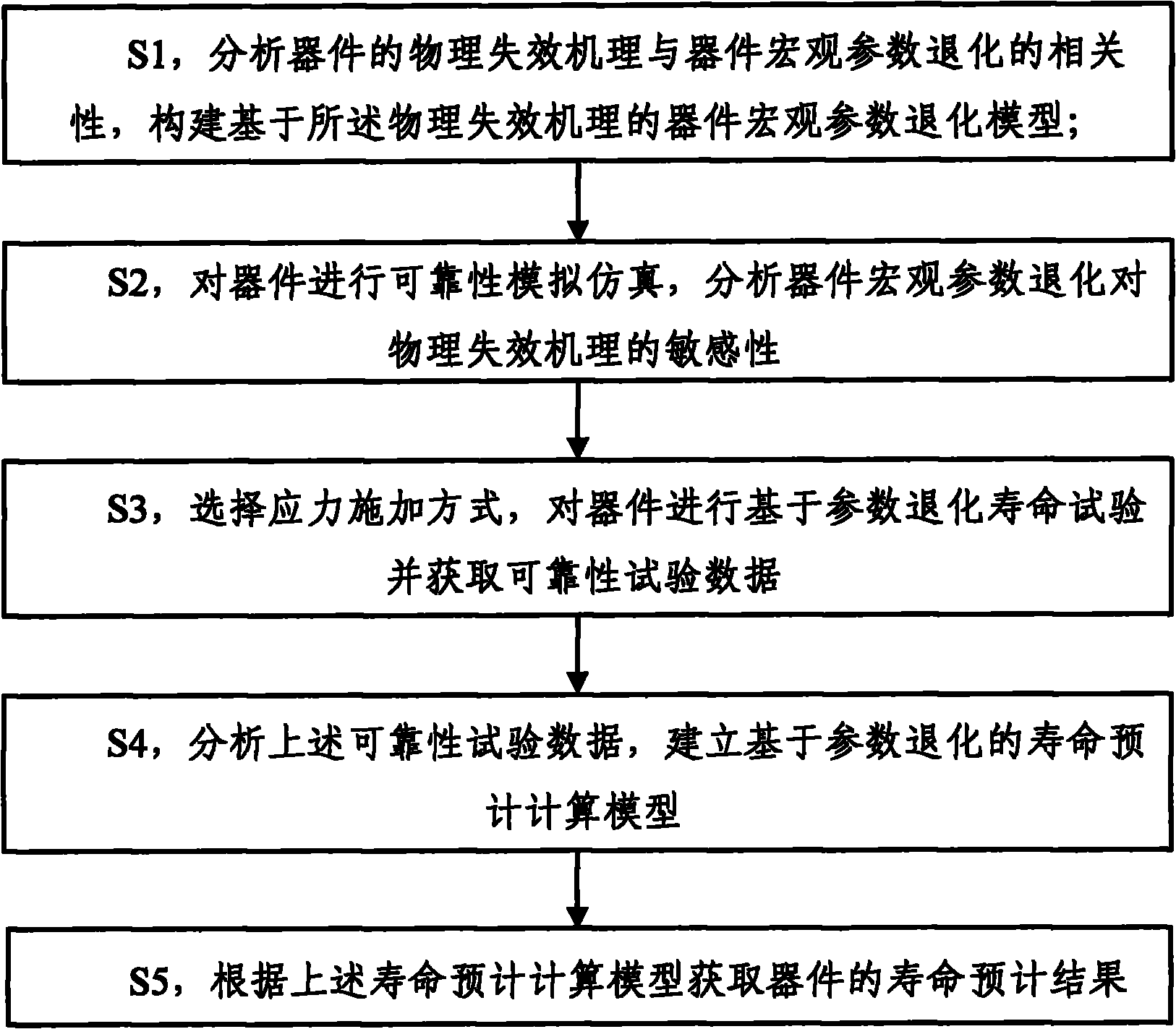
[0025] The specific implementation manners of the present invention will be further described in detail below in conjunction with the accompanying drawings and embodiments. The following examples are used to illustrate the present invention, but are not intended to limit the scope of the present invention.

[0026] The embodiment of the present invention aims at the physical failure mechanism of main MOS devices: HCI, TDDB, EM and NBTI, etc., analyzes the correlation between the failure mechanism of MOS devices and the degradation of device parameters, sorts out the macroscopic parameter degradation model of MOS devices based on physical failure; Technical experience and advanced software and hardware technical equipment in the field of testing and testing, design of high-precision and high-stability testing and testing platforms, combined with high-reliability, long-life integrated circuit design units, selection and processing of appropriate MOS devices and structures, design...


PUM


Abstract

The invention discloses a method for estimating service life of an MOS (Metal Oxide Semiconductor) device. The method comprises the steps of: analyzing the relevance of a physical failure mechanism and a device macroparameter degradation, constructing a device macroparameter degradation model based on the physical failure mechanism; carrying out reliability analog simulation on a device, analyzing the sensitivity of the device macroparameter degradation to the physical failure mechanism; selecting a stress applying mode, carrying out a parameter degradation service life-based test on the device and obtaining reliability test data; analyzing the reliability test data, establishing a parameter degradation-based service life estimating computing model; and obtaining a service life estimating result of the device according to the service life estimating computing model. By using the method, the problems of accuracy and maneuverability of the traditional device service life predicting method under the novel technical conditions are solved, the quantity of test samples is reduced, the testing cost is lowered, and the accuracy of predicting the testing result is improved.

Description

technical field [0001] The invention relates to the technical field of semiconductors, in particular to a MOS (Metal Oxid Semiconductor) device lifetime prediction method and system. Background technique [0002] my country's high-reliability and long-life integrated circuits are also facing challenges in reliability and testing while keeping up with the development of international semiconductor technology to achieve leapfrog progress in design and production. Highly reliable and long-life MOS devices have strict requirements for adaptability and stability in different environments, especially mutual adaptability. Therefore, high-reliability and long-life MOS devices put forward higher requirements for quality and reliability. [0003] On the other hand, with the advancement of technology, the failure rate of MOS devices, especially large-scale digital integrated circuits, has been significantly reduced compared with the past, and devices have almost no failure in the tradi...

Claims


Application Information

Patent Timeline
Patent Type & Authority Applications(China)
IPC IPC(8): G06F17/50
Inventor 王群勇阳辉钟征宇陈冬梅白桦刘燕芳吴文章陈宇
Owner BEIJING SHENGTAOPING TEST ENG TECH RES INST
Why Eureka
Try Eureka