Rapid annealing method for ohmic contact of metal and silicon carbide
What is AI technical title?
AI technical title is built by PatSnap AI team. It summarizes the technical point description of the patent document.
A rapid annealing, ohmic contact technology, used in electrical components, semiconductor/solid-state device manufacturing, circuits, etc., to achieve the effect of improving flexibility, improving quality, and increasing heating rate
Active Publication Date: 2012-07-11
NO 55 INST CHINA ELECTRONIC SCI & TECHNOLOGYGROUP CO LTD
View PDF2 Cites 11 Cited by
Summary
Abstract
Description
Claims
Application Information
AI Technical Summary
This helps you quickly interpret patents by identifying the three key elements:
Problems solved by technology
Method used
Benefits of technology
Problems solved by technology
The currently commonly used SiC rapid annealing method still has many defects, and the temperature control method in the heating process still needs to be improved.
Method used
Image
Click on the blue label to locate the original text in one second.
Reading with bidirectional positioning of images and text.
Examples
Embodiment 1
[0023] Referring to the accompanying drawings,
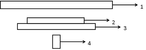
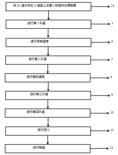
[0024] 1) Put the SiC wafer 2 on the Si wafer tray 3 and put it into the rapid heat treatment device 13, place the 3-inch 4H silicon carbide wafer (SiC wafer) 2 to be rapidly annealed on the 4-inch Si wafer tray 3, and then put it into the In the rapid heat treatment device 13, the heating surface 1 of the rapid annealing device is above the SiC wafer 2, the temperature measuring device 4 is below the Si wafer tray 3, and the protective gas Ar is filled at the same time;
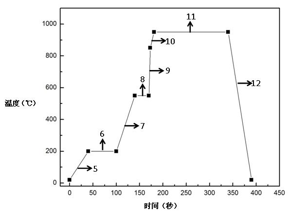
[0025] 2) The first heating stage 5, the temperature maintaining stage 6, the SiC wafer 2 is heated for the first time, heated to 200°C, which is the first temperature, maintained at the temperature for 60 seconds, and the heating rate is 5°C / s;
[0026] 3) In the second heating stage 7 and the temperature stabilization stage 8, the temperature of the SiC wafer 2 is raised for the second time, from 200°C to 550°C, which is the second temperature, the temperatu...
Embodiment 2
[0031] Referring to the accompanying drawings,
[0032] 1) Place the 2-inch 6H silicon carbide wafer (SiC wafer) 2 to be rapidly annealed on the 4-inch Si wafer 4, and then put it into the rapid heat treatment device 13. The heating surface 1 of the rapid annealing device is above the silicon carbide wafer. The temperature device 4 is below the Si chip tray 3, filled with protective gas N2;
[0033] 2) The first heating stage 5, the temperature maintaining stage 6, the SiC wafer 2 is heated for the first time, heated to 300°C, which is the first temperature, kept for 180 seconds, and the heating rate is 10°C / s;
[0034] 3) In the second heating stage 7 and the temperature stabilization stage 8, the temperature of the SiC wafer 2 is raised for the second time, from 200°C to 600°C, which is the second temperature, the temperature is stabilized for 60 seconds, and the heating rate is 20°C / s;
[0035] 4) In the third heating stage 9, the SiC wafer 2 is heated for the third time, ...
PUM
Property
Measurement
Unit
thickness
aaaaa
aaaaa
Abstract
The invention provides a rapid annealing method for ohmic contact of metal and siliconcarbide, which comprises the steps of (1) placing SiC wafers on a Si sheet tray, then arranging the Si sheet tray on a rapid thermal treatment device, and simultaneously filling the device with protection gas Ar; (2) performing a first temperature-rise period, and keeping the temperature; (3) performing a second temperature-rise period, and steadying the temperature; (4) performing a third temperature-rise period; (5) performing a fourth temperature-rise period, namely, annealing period; and (6) performing a temperature reducing period. The method has benefits as follows: the method is carried out in the commercial rapid thermal treatment device taking any light radiation as a heat source; and the silicon sheet used as the tray can adopt various standards of commercial polishingmonocrystalline silicon sheets and has low cost. The annealing method can remove the moisture on the surface of the siliconcarbidewafer and stabilize the temperature. On the premise of ensuring the control precision of the peak thermal treatment temperature, the heating rate is improved through changing the setting value. Finally, the annealed ohmic contact resistance is reduced; and the quality of the ohmic contact, the device reliability and the yield are improved.
Description
technical field [0001] The invention relates to a rapid annealing method, in particular to a metal-silicon carbide ohmic contact rapid annealing method. Background technique [0002] Siliconcarbide (SiC) material is the third-generation wide-bandgap semiconductor material developed after the first-generation elemental semiconductor material (Si) and the second-generation compound semiconductor material (GaAs, GaP, InP, etc.). Due to the characteristics of wide band gap, high critical breakdown electric field, high thermal conductivity, and high electron saturation drift velocity, SiC materials are especially suitable for making microwave high-power, high-voltage, high-temperature, and radiation-resistant electronic devices, and have a wide range of applications in all aspects of the national economy. application. At present, the development of SiC devices has become a research hotspot. [0003] One of the key processes in the preparation of SiC devices is to realize the o...
Claims
Application Information
Patent Timeline
Application Date:The date an application was filed.
Publication Date:The date a patent or application was officially published.
First Publication Date:The earliest publication date of a patent with the same application number.
Issue Date:Publication date of the patent grant document.
PCT Entry Date:The Entry date of PCT National Phase.
Estimated Expiry Date:The statutory expiry date of a patent right according to the Patent Law, and it is the longest term of protection that the patent right can achieve without the termination of the patent right due to other reasons(Term extension factor has been taken into account ).
Invalid Date:Actual expiry date is based on effective date or publication date of legal transaction data of invalid patent.
Patent Type & AuthorityApplications(China)
IPC IPC(8): H01L21/04H01L21/28
Inventor李理柏松陈刚
OwnerNO 55 INST CHINA ELECTRONIC SCI & TECHNOLOGYGROUP CO LTD

