Preparation method for Schottky diode based on core/shell structure silicon nanowire set

A Schottky diode and silicon nanowire technology, applied in the field of semiconductor materials and nano-devices, can solve the problems of harsh preparation conditions, high cost, high repeatability, etc., and achieve the effect of simple preparation method, low cost and high repeatability

Inactive Publication Date: 2012-07-18
EAST CHINA NORMAL UNIV
View PDF3 Cites 4 Cited by
  • Summary
  • Abstract
  • Description
  • Claims
  • Application Information

AI Technical Summary

Problems solved by technology

[0006] The object of the present invention is to provide a method for preparing a Schottky diode based on a core / shell structure silicon nanowire group, to solve the existing problems of harsh preparation conditions and high cost of the Schottky diode based on a silicon nanowire group, and to provide a Low-cost, high-reproducibility, new method suitable for large-scale industrial production

Method used


Image

  • Preparation method for Schottky diode based on core/shell structure silicon nanowire set
  • Preparation method for Schottky diode based on core/shell structure silicon nanowire set
  • Preparation method for Schottky diode based on core/shell structure silicon nanowire set

Examples


Embodiment

[0031] 1) Wafer cleaning

[0032] Take a 1cm×1cm silicon wafer (p-type, double-sided polishing, crystal orientation, resistivity 0.1-10Ω·cm), clean the silicon wafer with standard RCA cleaning steps and dry it with nitrogen gas for later use.

[0033] 2) Al back electrode preparation

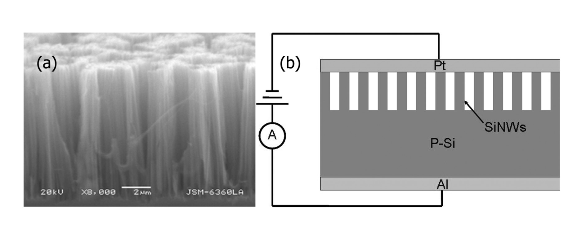
[0034] Evaporate Al on one side of the silicon wafer by a vacuum evaporation device, and thermally anneal at 450°C for 5 minutes in a nitrogen atmosphere to form a good ohmic contact Al back electrode; spin-coat the Al back electrode surface with photoresist, dry the photoresist, In order to protect the back electrode from being damaged during the preparation of the silicon nanowire by the electroless chemical etching method.

[0035] 3) Preparation of silicon wafer chemical etching solution

[0036] Prepare 25 mmol L -1 AgNO 3 , hydrofluoric acid (40% HF concentration) mixed solution (25 mmol L -1 AgNO 3 and concentration of 40% HF volume ratio (1:1) 200 mL, sonicate to make the mixed so...


PUM

PropertyMeasurementUnit
electrical resistivityaaaaaaaaaa

Abstract

The invention discloses a preparation method for a Schottky diode based on a core / shell structure silicon nanowire set. The method comprises the following steps of: silicon slice cleaning, back electrode preparation, silicon nanowire preparation, silicon nanowire gap filling, Pt thin-film deposition and the like. Silicon nanowires of the Schottky diode are of core / shell structures; silicon is a core; and a surface oxidation layer is a shell. When the Schottky diode is applied, the surface oxidation layer does not need to be removed. A current transmission mechanism of the prepared Schottky diode is a trap-assisted tunneling mechanism, so that the Schottky diode has an excellent rectification characterisitic and has a broad application prospect in the field of nanodevices and the field of new energy resources. The preparation method for the Schottky diode based on the core / shell structure silicon nanowire set is simple, is friendly to the environment, is low in cost requirement and is high in repeatability and is suitable for large-scale industrial production.

Description

technical field [0001] The invention relates to the technical fields of semiconductor materials and nano devices, in particular to a method for preparing a Schottky diode based on a core / shell structure silicon nanowire group. technical background [0002] Schottky diodes have favorable properties in many applications compared to other types of diodes: (1) lower turn-on voltage; (2) shorter recovery time; (3) lower junction capacitance. Schottky diodes are widely used as diode rectifiers in RF mixers and detectors, power rectifiers, integrated power supplies or circuits, solar cells and fuel cells, etc. [0003] Silicon nanowire is a typical representative of one-dimensional nanomaterials. In addition to the properties of bulk silicon, it also shows physical properties different from bulk silicon, such as field emission, thermal conductivity, and photoluminescence. It is used in nanoelectronic devices, Optoelectronic devices and new energy have great potential application v...

Claims


Application Information

Patent Timeline
Patent Type & Authority Applications(China)
IPC IPC(8): H01L21/329
Inventor 王志亮陈雪皎朱美光陈云严强张健
Owner EAST CHINA NORMAL UNIV
Why Eureka
Try Eureka