

Super junction device with multiple embedded P islands and N channels and preparation method thereof
A superjunction device and channel technology, applied in semiconductor/solid-state device manufacturing, semiconductor devices, electrical components, etc., can solve the problem of uneven electric field distribution in the drift region, and achieve the effect of solving uneven electric field distribution
- Summary
- Abstract
- Description
- Claims
- Application Information
AI Technical Summary
Problems solved by technology
Method used
Image

Examples
Embodiment 1
[0045] The invention provides a method for preparing an N-channel superjunction device with embedded multi-P islands. The method includes the following steps:
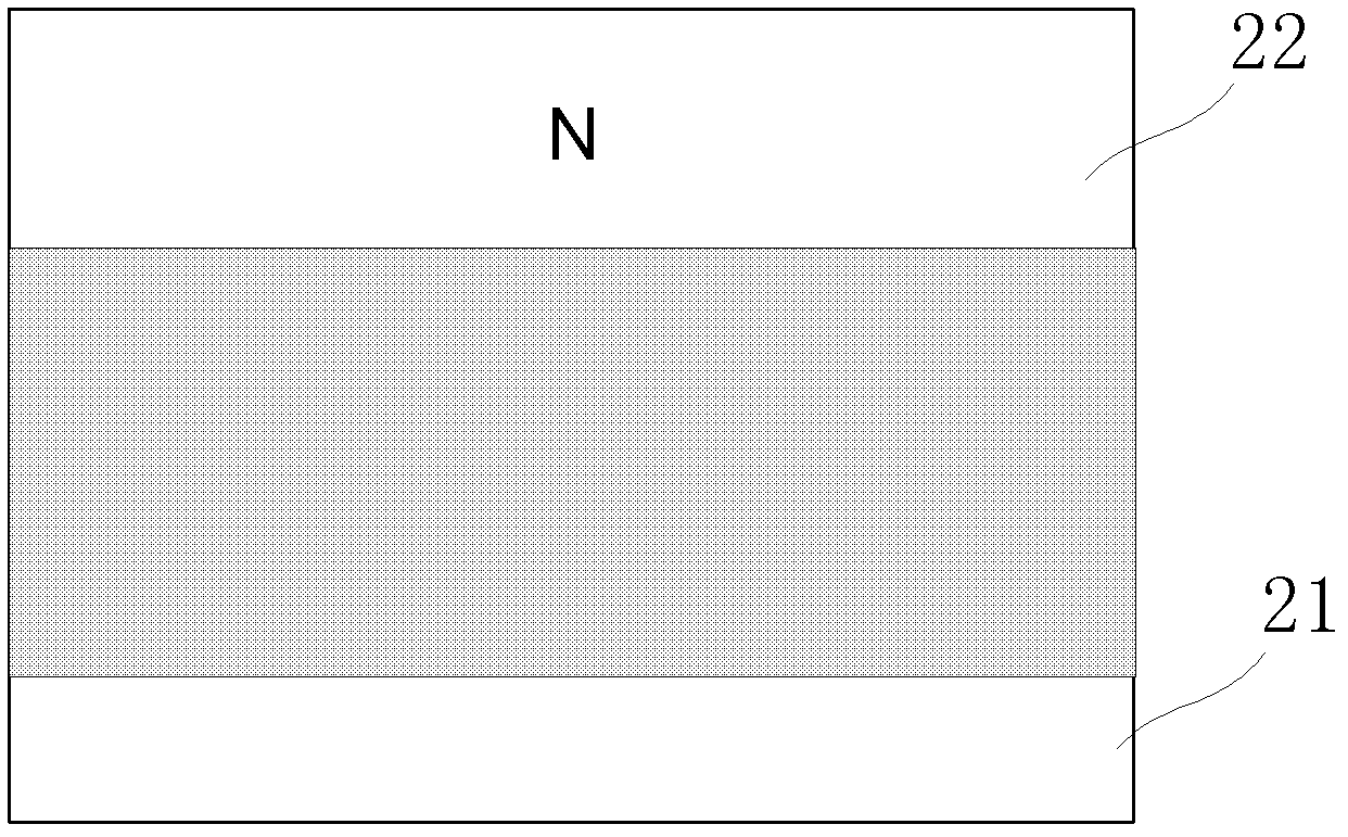
[0046] In step 1), a semiconductor substrate 21 is provided, and a layer of N-type drift region 22 is prepared on the semiconductor substrate 21 by N-type ion implantation; specifically, the semiconductor substrate 21 is a bulk silicon substrate or SOI substrate. see figure 2 , as shown in the figure, in this embodiment, the semiconductor substrate 21 is an SOI substrate as an example for illustration, and the N-type drift region 22 is formed in the top silicon layer of the SOI substrate, specifically, in N-type ions of group V elements (such as phosphorus, arsenic, antimony, etc.) are doped into the top silicon of the SOI substrate to replace the positions of silicon atoms in the crystal lattice to form an N-type drift region 22 .
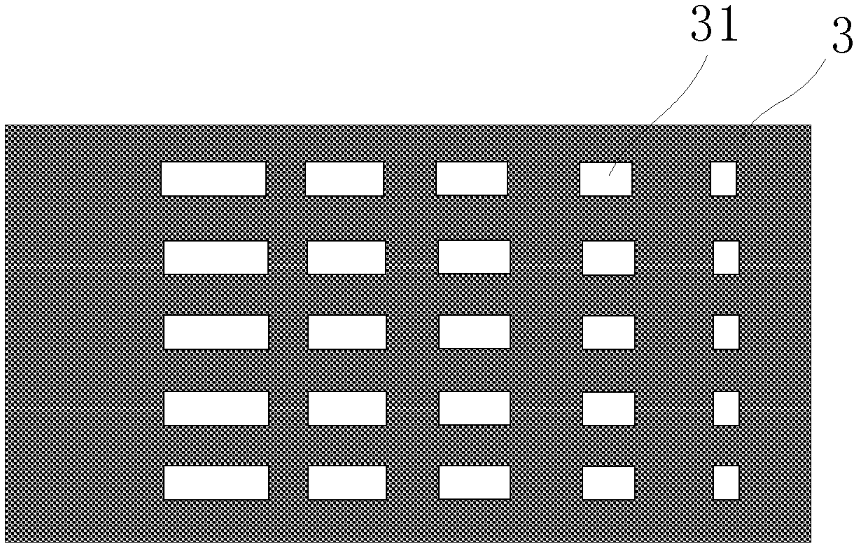
[0047] Then, provide a mask plate 3 with multiple groups of ion implantation window...
Embodiment 2
[0052] This embodiment is the same as step 1) and step 4) in the above-mentioned embodiment 1, so it will not be described in detail. In step 2 in this embodiment, boron ions are implanted into the N-type drift region 22 repeatedly and borrowed The concentration distribution of boron ions is controlled by the shielding of the mask plate 3, and annealed in step 3), and then a plurality of mutually spaced and horizontally parallel and longitudinally parallel arrangements can be formed in the N-type drift region 22. The island-shaped P region 23, as shown in Figure 7 shown.
Embodiment 3
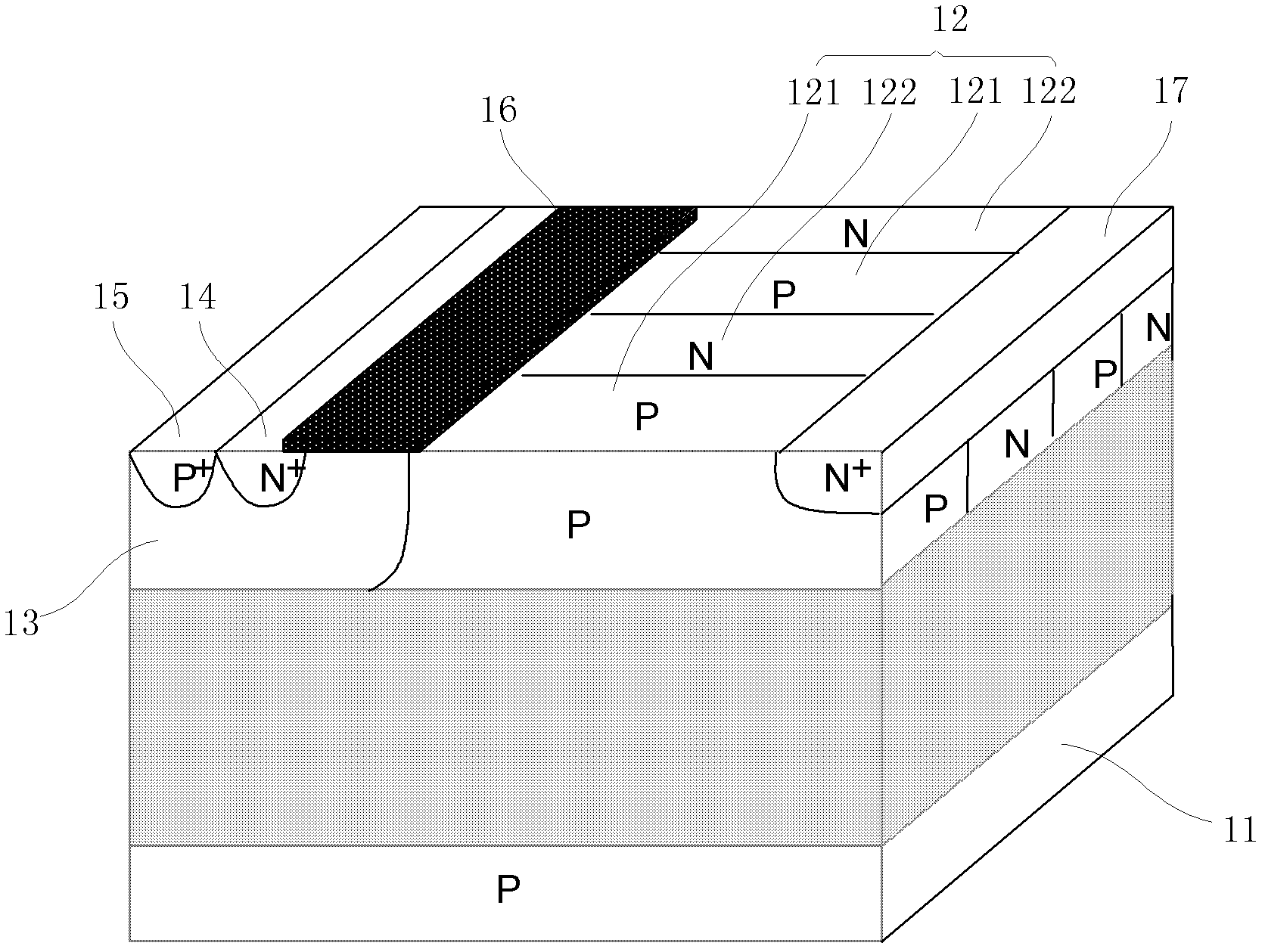
[0054] The present invention also provides an embedded multi-P-island N-channel superjunction device, please refer to Figure 6 , which is a schematic diagram showing the structure of an embedded multi-P island N-channel superjunction device according to the present invention. As shown in the figure, the embedded multi-P-island N-channel superjunction device includes: a semiconductor substrate 21 formed on the semiconductor substrate The N-type drift region 22 on the bottom 21, the P-type body region 24 on one side of the N-type drift region 22, and the N-type drain region 28 on the other side of the N-type drift region 22, the P The body 24 includes an N-type source region 25 , a P-type body contact region 27 and a gate oxide layer 27 .
[0055] A plurality of island-shaped P regions 23 are formed in the N-type drift region 22 , and each of the island-shaped P regions 23 linearly decreases from the N-type source region 25 to the N-type drain region 28 . The semiconductor sub...
PUM
 Abstract
Description
Claims
Application Information