Method for preparing resistive random access memory

A resistive variable memory and resistive variable technology, applied in the direction of static memory, digital memory information, information storage, etc., can solve the problems of obvious parasitic effects of devices and incomplete isolation between devices, so as to reduce process complexity and ensure The effect of complete isolation and great application prospects

Inactive Publication Date: 2012-07-18
PEKING UNIV
View PDF7 Cites 5 Cited by
  • Summary
  • Abstract
  • Description
  • Claims
  • Application Information

AI Technical Summary

Problems solved by technology

[0005] However, based on the traditional sputtering and deposition three-layer MIM process, due to the full coverage of the middle dielectric layer, the dielectric layer between the bottom electrode and the top electrode is completely connected, and the actual size of the device is much larger than the design size. The device is not completely isolated from each other, and the parasitic effect of the device is obvious

Method used


Image

  • Method for preparing resistive random access memory
  • Method for preparing resistive random access memory
  • Method for preparing resistive random access memory

Examples


Embodiment 1

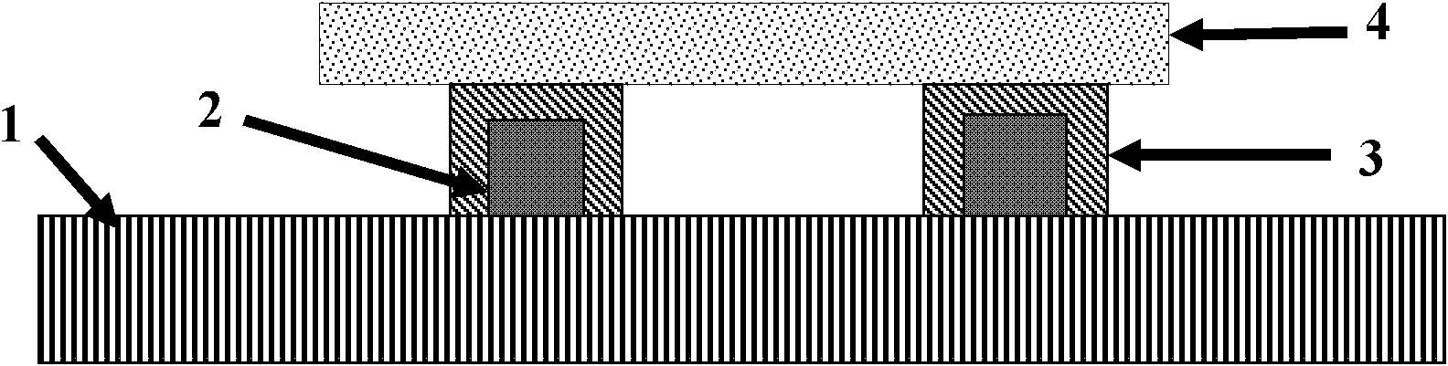
[0025] The schematic diagram of the cross-sectional structure of the resistive memory made in this embodiment is as follows: figure 1 As shown, the preparation process of the resistive memory in this embodiment is described below in combination with the schematic cross-sectional structure:

[0026] 1) First, on the silicon substrate 1, a layer of Ta metal 200nm is prepared by using a physical vapor deposition (PVD) method or a film-forming method in other IC processes;

[0027] 2) Using standard photolithography and lift-off techniques to pattern the bottom electrode to form the bottom electrode 2;

[0028] 3) Using dry oxygen oxidation method, in a high-temperature oxidation furnace, oxidize at 400°C for 2 hours to form a 10nm TaOx (X=1-2.5) film wrapped around the bottom electrode;

[0029] 4) Define the bottom electrode lead-out hole by photolithography and etching;

[0030] 5) Same as the preparation of the bottom electrode, the top electrode TiN and its protective elect...

Embodiment 2

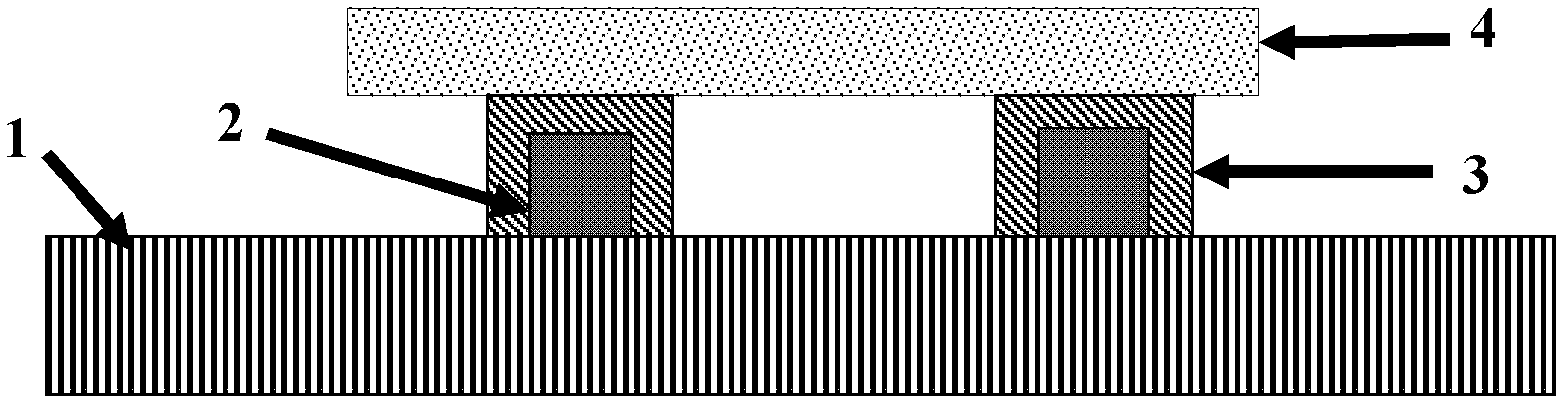
[0035] 1) First, a layer of W metal 200nm is prepared on the silicon substrate 1 by using a physical vapor deposition (PVD) method or a film-forming method in other IC processes;

[0036] 2) Using standard photolithography and lift-off techniques to pattern the bottom electrode to form the bottom electrode;

[0037] 3) Using the wet oxygen oxidation method, oxidize in an oxidation furnace at 400°C for 3 hours to form a 10nm WOx film (X=1-3) wrapped around the bottom electrode;

[0038] 4) Define the bottom electrode lead-out hole by photolithography and etching;

[0039] 5) Same as the preparation of the bottom electrode, the top electrode TiN and its protective electrode Pt are prepared by PVD method or other film-forming methods in the IC process.

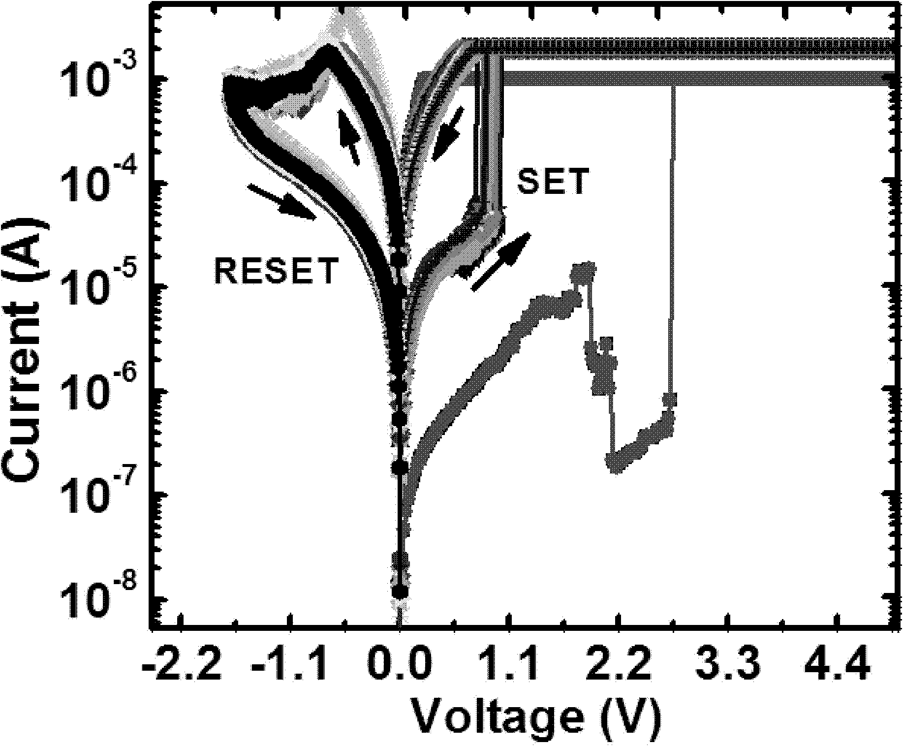
[0040] The resistive change memory (W / WOx / Cu) prepared in this embodiment has similar resistive change characteristics, erasable characteristics and retention characteristics at high temperature as that of the resistive change m...


PUM

PropertyMeasurementUnit
thicknessaaaaaaaaaa
thicknessaaaaaaaaaa

Abstract

The invention discloses a method for preparing a resistive random access memory. The method comprises the following steps: preparing a bottom electrode on a substrate; then, carrying out partial oxidation on the metal of the bottom electrode so as to form a metal oxide with a thickness of 3-50 nm, and taking the metal oxide as a resistive random material layer; and finally, preparing a top electrode on the resistive random material layer. By using the method disclosed by the invention, a step of depositing a resistive random material layer in the traditional method is avoided, thereby greatly reducing the process complexity; meanwhile, the self-alignment between the resistive random material layer and the bottom electrode can be realized; the complete isolation between devices is ensured; various parasitic effects generated by the traditional process methods are avoided; and the consistency of the actual area and design area of each device is ensured.

Description

technical field [0001] The invention belongs to the technical field of ultra-large-scale integrated circuits, and in particular relates to a preparation method of a non-volatile resistive memory device. Background technique [0002] With the continuous advancement of integrated circuit technology, the FLASH technology based on the traditional floating gate structure will face technical challenges that cannot be scaled down proportionally. In recent years, the resistive RAM (RRAM) based on the MIM (Metal-Insulator-Metal) structure has attracted much academic attention due to its simple structure, easy fabrication, small size, high integration, fast erasing and writing speed, and low power consumption. world and industry attention. Different from FLASH of the traditional floating gate structure, which relies on the amount of charge to store information 0 and 1, RRAM utilizes its high resistance and low resistance states under different electrical conditions to store informati...

Claims


Application Information

Patent Timeline
Patent Type & Authority Applications(China)
IPC IPC(8): H01L45/00
CPCG11C2213/15H01L45/00G11C11/56G11C2013/0073G11C13/0007H10N70/20H10N70/826H10N70/028H10N70/8833
Inventor 黄如谭胜虎张丽杰潘岳黄英龙杨庚宇唐昱毛俊蔡一茂
Owner PEKING UNIV
Why Eureka
Try Eureka