Device and method for measuring three-dimensional distribution of residual stress in metal microstructure
A technology of metal microstructure and residual stress, applied in the direction of material analysis using radiation diffraction, etc., can solve the problems of poor measurement accuracy, large workload, inability to carry out, etc. Effect
- Summary
- Abstract
- Description
- Claims
- Application Information
AI Technical Summary
Problems solved by technology
Method used
Image
Examples
Embodiment
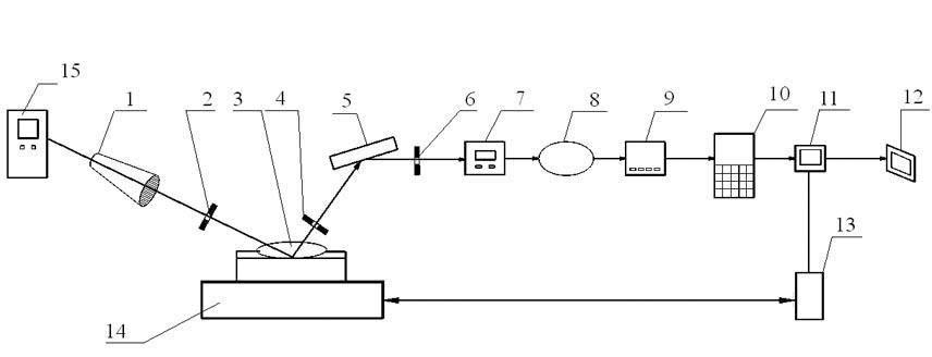
[0034] Such as figure 1 A device for measuring the three-dimensional distribution of residual stress in metal microstructures shown includes: an X-ray generating system, a micro-diffraction and optical path guiding system, a workbench system, a detection system, a computer and a control system. The X-ray tube in the X-ray generating system is a short-wavelength X-ray tube, and the anode target is made of copper, or molybdenum, or A9, or tungsten; a synchrotron radiation source 15 is used in the X-ray generating system. The micro-diffraction and optical path guiding system includes: the micro-diffraction and optical path guiding system includes: a tapered capillary 1, an exit slit 2, an anti-scattering slit 4, a plane monochromator 5 and a receiving slit 6; the detection system includes : detector 7, amplifier 8, pulse height analyzer 9, counter 10; the workbench system is a precision three-dimensional platform with grating that can move in X, Y and Z three-dimensional directio...
PUM
 Abstract
Description
Claims
Application Information

