

Manufacturing method for double-face illuminated crystalline silicon solar cell
A technology of solar cells and crystalline silicon, applied in the field of solar cells, can solve the problems of high recombination rate of aluminum back field surface, restricted efficiency improvement, complicated process, etc., and achieves the improvement of photoelectric conversion efficiency, simplified operation and simple preparation method. Effect
- Summary
- Abstract
- Description
- Claims
- Application Information
AI Technical Summary
Problems solved by technology
Method used
Image

Examples
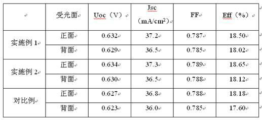
Embodiment 1
[0040] A method for preparing a double-sided light-receiving crystalline silicon solar cell, comprising the steps of:
[0041] (1) Clean the original silicon wafer to remove the damaged layer on the back to form a polished surface; the other side (front) remains in its original state;
[0042] (2) Put the fronts of the silicon wafers back to back into the diffusion furnace for boron diffusion, and the back of the silicon wafers is the diffusion surface;
[0043] (3) Deposit a SiN mask layer on the back of the diffused silicon wafer;
[0044] (4) Clean the front side of the silicon wafer, put the silicon wafer into the lye to remove the damaged layer and make texture, so that the other side (front side) of the silicon wafer forms a textured surface, and remove the diffusion diffraction layer at the same time;
[0045] (5) Put the back of the silicon wafer back to back into the diffusion furnace for single-sided phosphorus diffusion, and the front of the silicon wafer is the di...
Embodiment 2
[0051] A method for preparing a double-sided light-receiving crystalline silicon solar cell, comprising the steps of:
[0052] (1) Clean the original silicon wafer to remove the damaged layer on the back to form a polished surface; the other side (front) remains in its original state;
[0053] (2) Put the fronts of the silicon wafers back to back into a diffusion furnace for phosphorus diffusion, and the back of the silicon wafers is the diffusion surface;
[0054] (3) Deposit a SiN mask layer on the back of the diffused silicon wafer;
[0055] (4) Clean the front side of the silicon wafer, put the silicon wafer into the lye to remove the damaged layer and make texture, so that the other side (front side) of the silicon wafer forms a textured surface, and remove the diffusion diffraction layer at the same time;
[0056] (5) Put the back of the silicon wafer back to back into the diffusion furnace for single-sided boron diffusion, and the front of the silicon wafer is the diff...
PUM
 Abstract
Description
Claims
Application Information