Solar cell manufacturing method and solar cell
A solar cell and manufacturing method technology, applied to circuits, photovoltaic power generation, electrical components, etc., can solve the problems of complicated photolithography process steps and high cost, and achieve the effects of improving service life, reducing costs, and simplifying process steps
- Summary
- Abstract
- Description
- Claims
- Application Information
AI Technical Summary
Problems solved by technology
Method used
Image

Examples
Embodiment 1
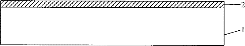
[0056] refer to figure 1 , step S 1 . Forming an N+ type doped layer 2 on the surface of the N type substrate 1 , the sheet resistance of the N+ type doped layer is 20Ω / □. Specifically, phosphorus ions are accelerated to 500eV and the phosphorus ions are implanted into the N-type substrate from the surface of the N-type substrate by means of ion implantation.
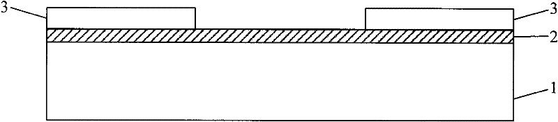
[0057] refer to figure 2 , step S 2 1. Forming a patterned thin film 3 on the surface of the N+ type doped layer 2, wherein the area not covered by the patterned thin film 3 is an open area; the patterned thin film acts as a mask. The patterned film 3 is formed by screen printing, wherein the patterned film has a thickness of 1 μm and is made of synthetic rubber. After the patterned film is formed, the film is dried.
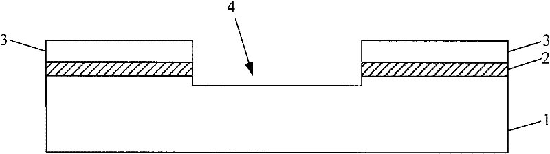
[0058] refer to image 3 , step S 3 1. Etching the open area, the etching depth is greater than the thickness of the N+ type doped layer 2 and up to the N-type substrate 1, in this embodiment, th...
Embodiment 2
[0065] refer to figure 1 , step S 1 . Forming an N+ type doped layer 2 on the surface of the N type substrate 1 , the sheet resistance of the N+ type doped layer is 100Ω / □. Specifically, phosphorus ions are accelerated to 50keV and the phosphorus ions are implanted into the N-type substrate from the surface of the N-type substrate by means of ion implantation.
[0066] refer to figure 2 , step S 2 1. Forming a patterned thin film 3 on the surface of the N+ type doped layer 2, wherein the area not covered by the patterned thin film 3 is an open area; the patterned thin film acts as a mask. The patterned film 3 is formed by screen printing, wherein the patterned film has a thickness of 50 μm and is made of copper-aluminum alloy. After the patterned film is formed, the film is dried.
[0067] refer to image 3 , step S 3 1. Etching the open area, the etching depth is greater than the thickness of the N+ type doped layer 2 and reaches the N-type substrate 1. In this embod...
Embodiment 3
[0074] refer to figure 1 , step S 1 . Forming an N+ type doped layer 2 on the surface of the N type substrate 1 , the sheet resistance of the N+ type doped layer is 60Ω / □. Specifically, phosphorus ions are accelerated to 30keV and the phosphorus ions are implanted into the N-type substrate from the surface of the N-type substrate by means of ion implantation.
[0075] refer to figure 2 , step S 2 1. Forming a patterned thin film 3 on the surface of the N+ type doped layer 2, wherein the area not covered by the patterned thin film 3 is an open area; the patterned thin film acts as a mask. The patterned film 3 is formed by screen printing, wherein the patterned film has a thickness of 30 μm and is made of copper-aluminum alloy. After the patterned film is formed, the film is dried.
[0076] refer to image 3 , step S 3 1. Etching the open area, the etching depth is greater than the thickness of the N+ type doped layer 2 and reaches the N-type substrate 1. In this embodi...
PUM
| Property | Measurement | Unit |
|---|---|---|
| thickness | aaaaa | aaaaa |
| thickness | aaaaa | aaaaa |
| thickness | aaaaa | aaaaa |
Abstract
Description
Claims
Application Information
 - R&D
- Intellectual Property
- Life Sciences
- Materials
- Tech Scout
- Unparalleled Data Quality
- Higher Quality Content
- 60% Fewer Hallucinations
Browse by: Latest US Patents, China's latest patents, Technical Efficacy Thesaurus, Application Domain, Technology Topic, Popular Technical Reports.
© 2025 PatSnap. All rights reserved.Legal|Privacy policy|Modern Slavery Act Transparency Statement|Sitemap|About US| Contact US: help@patsnap.com