Preparation method of low-temperature polycrystalline silicon film and low-temperature polycrystalline silicon film

A low-temperature polysilicon and polysilicon growth technology, used in transistors, semiconductor/solid-state device manufacturing, electrical components, etc., can solve problems such as affecting the current characteristics of polysilicon thin film transistors, and achieve the effect of improving current characteristics and low surface roughness.

Inactive Publication Date: 2012-08-29
BOE TECH GRP CO LTD
View PDF15 Cites 27 Cited by
  • Summary
  • Abstract
  • Description
  • Claims
  • Application Information

AI Technical Summary

Problems solved by technology

[0006] The technical problem to be solved by the present invention is to provide a method for preparing a low-temperature polysilicon thin film for t

Method used


Image

  • Preparation method of low-temperature polycrystalline silicon film and low-temperature polycrystalline silicon film
  • Preparation method of low-temperature polycrystalline silicon film and low-temperature polycrystalline silicon film
  • Preparation method of low-temperature polycrystalline silicon film and low-temperature polycrystalline silicon film

Examples


Embodiment 1

[0041] In this embodiment, the following steps are used to prepare a low-temperature polysilicon thin film:

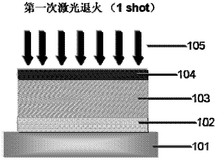
[0042] (1) Forming a buffer layer on the substrate: the substrate 101 is a glass substrate, and after the glass substrate is pre-cleaned, a double-layer structure SiN is deposited by plasma-enhanced chemical vapor deposition (PECVD) x / SiO 2 The thin film is used as an insulating buffer layer, first depositing a 100nm silicon nitride layer 102, and then depositing a 200nm silicon dioxide layer 103;

[0043] (2) Forming an amorphous silicon layer of 30-100 nm on the insulating buffer layer obtained in step (1): depositing an amorphous silicon layer 104 of 60 nm;

[0044] (3) Perform high-temperature treatment on the amorphous silicon layer obtained in step (2): at a temperature of 450° C., perform high-temperature treatment on the amorphous silicon layer 104 for 2 hours;

[0045] (4) The first laser annealing treatment is carried out on the amorphous silicon layer, so...

Embodiment 2

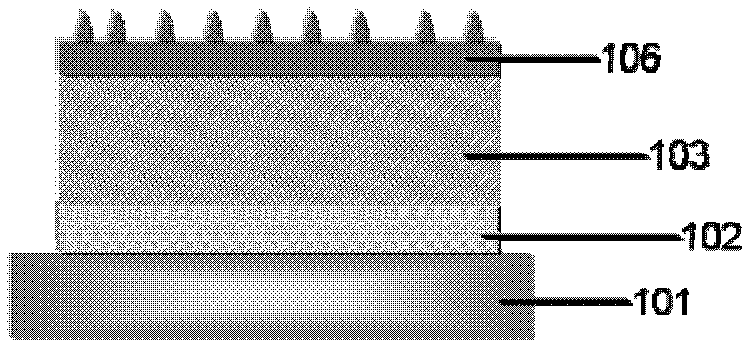
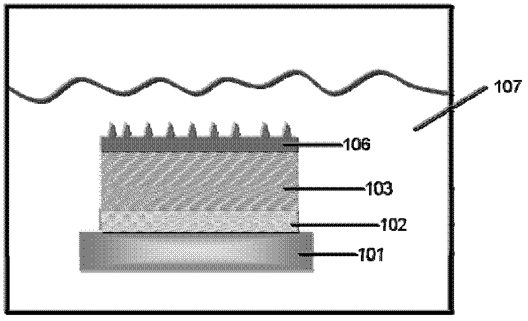
[0050] The main method steps are the same as in Example 1, except that the etching solution 107 in step (4) is cleaned with a concentration of 1 wt% dichromic acid solution, and the etching time is 60s; step (6) adopts 39 shots (shooting times) Perform the second annealing treatment 109, select the laser linear beam width to be 400 μm, the laser pulse frequency to be 300 Hz, and the laser energy density to be 400 mJ / cm 2 , the scanning speed is 2mm / s, and the pulse width is 25 nanoseconds. The surface of the obtained polysilicon film was detected by an atomic force microscope (AFM), and the highest protrusion was only about 20 nm.

[0051] Figure 7 It is a schematic cross-sectional view of a polysilicon film 111 obtained in the prior art. It can be seen that the protrusions at the grain boundaries are very obvious, and are generally substances with high resistance (the combination of silicon-silicon valence bonds and partial oxides that have a distorted crystal lattice). , ...


PUM

PropertyMeasurementUnit
Thicknessaaaaaaaaaa
Thicknessaaaaaaaaaa
Thicknessaaaaaaaaaa

Abstract

The invention provides a preparation method of a low-temperature polycrystalline silicon film. According to the method, a buffer layer and a noncrystalline silicon layer are firstly formed on a base plate, then, primary laser annealing treatment is carried out on the noncrystalline silicon layer so that the noncrystalline silicon layer is converted into a polycrystalline silicon growth bottom layer, next, the polycrystalline silicon growth bottom layer is subjected to etching treatment so that the surface of the polycrystalline silicon growth bottom layer obtained in the primary laser annealing treatment gradually becomes flat, subsequently, the polycrystalline silicon growth bottom layer is subjected to secondary annealing treatment, and the polycrystalline silicon film is obtained. The surface roughness of the low-temperature polycrystalline silicon film prepared by the method is low, and the current characteristics of subsequently prepared polycrystalline silicon film transistors are good.

Description

technical field [0001] The invention relates to a method for preparing a thin film, in particular to a method for preparing a low-temperature polysilicon thin film and the low-temperature polysilicon thin film. Background technique [0002] Organic light-emitting display (OLED) has attracted much attention due to its many advantages such as self-illumination, fast response, thinness, low power consumption and flexible display, and is considered to be the next generation of flat panel display technology. At present, OLED technology has been gradually applied to various electronic products, among which the active matrix organic light-emitting display (AMOLED) is famous for its advantages of high image quality, short response time of moving images, low power consumption, wide viewing angle and ultra-light and ultra-thin. Become the main trend of OLED development. [0003] At present, polysilicon thin film transistors are mostly used in AMOLED backplane technology, and polysili...

Claims


Application Information

Patent Timeline
IPC IPC(8): H01L21/20H01L21/268H01L21/336H01L29/786
Inventor 田雪雁龙春平姚江峰
Owner BOE TECH GRP CO LTD
Why Eureka
Try Eureka