Multi-layer tunnel cascaded semiconductor laser

A laser and semiconductor technology, applied in the structure of optical waveguide semiconductor and the structure of active area, etc., can solve the problems of reduced light extraction efficiency and power, high tunnel junction resistance and voltage, large divergence angle, etc., to improve the output optical power. , the internal resistance and its pressure drop are reduced, and the effect of high economic efficiency

Active Publication Date: 2015-08-19
THE 13TH RES INST OF CHINA ELECTRONICS TECH GRP CORP
View PDF0 Cites 0 Cited by
  • Summary
  • Abstract
  • Description
  • Claims
  • Application Information

AI Technical Summary

Problems solved by technology

In the past, tunnel junctions worked hard to increase the doping concentration. Although the resistance can be reduced, the diffusion of electrons and holes will absorb light, reducing the light extraction efficiency and power.
In addition, the previous tunnel cascade lasers have problems such as optical field overlap, high resistance and voltage of the tunnel junction, and large divergence angle.

Method used


Image

  • Multi-layer tunnel cascaded semiconductor laser
  • Multi-layer tunnel cascaded semiconductor laser
  • Multi-layer tunnel cascaded semiconductor laser

Examples


Embodiment 1

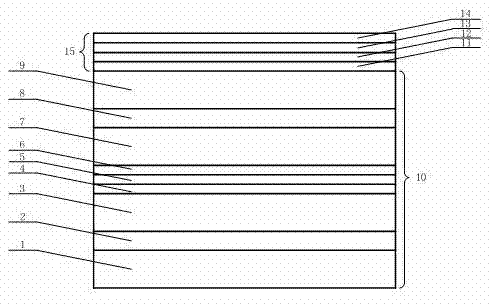
[0025] Depend on figure 1 It can be seen that the multi-layer tunnel cascaded semiconductor laser includes three vertically connected single-layer laser units 10 with the same structure; two adjacent single-layer laser units 10 pass through tunnel junctions with special structures according to semiconductor crystal growth rules. The unit 15 is grown and connected; the tunnel junction unit 15 includes a highly doped PN junction and a highly doped superlattice layer regularly grown on the upper and lower sides of the PN junction; the superlattice layer includes a semiconductor crystal The P-type superlattice layer 11 and the N-type superlattice layer 14 on the upper side of the P-type superlattice layer 14 that growth rule grows in the highly doped PN junction; N-type semiconductor layer 13 formed by doping technology.

[0026] In this embodiment, 11-14 form a tunnel junction unit 15 with a special structure. The single-layer laser unit 10 is a 900nm semiconductor laser, and t...

Embodiment 2

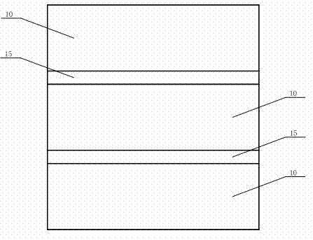
[0039] Depend on Figure 6 and Figure 7 As we know, the difference from Embodiment 1 is that this embodiment consists of two single-layer laser units 10—the first single-layer laser unit 16 and the second single-layer laser unit 18, and these two laser units pass through a tunnel with a special structure. The junction unit 15 is connected.

[0040] The structures of these two single-layer laser units 10 are different, the first single-layer laser unit 16 is a 940nm semiconductor laser, the second single-layer laser unit 18 is a 980nm semiconductor laser, and the level distribution of the second single-layer laser unit 18 is the same as in the embodiment The layer distribution of the single-layer laser unit 10 (900nm semiconductor laser) in 1 is the same, but the layer distribution of the first single-layer laser unit 16 is different from that of the single-layer laser unit 10 in Embodiment 1. The biggest difference is that the above The cladding layer and the lower cladding...


PUM


Abstract

The invention discloses a multi-overlaid layer tunnel cascaded semiconductor laser, which belongs to the field of semiconductor lasers. The multi-overlaid layer tunnel cascaded semiconductor laser comprises 2-4 single-layer laser units which are connected vertically, wherein two adjacent single-layer laser units are connected with each other by growing a tunnel junction unit layer with a special structure according to a semiconductor crystal growing rule; and a tunnel joint unit comprises a highly-doped PN junction and a super lattice layer which grows on the upper side or / and lower side of the PN junction regularly. The tunnel cascaded semiconductor laser is formed by a special tunnel junction with a super lattice, so that the output light power of the semiconductor laser is greatly increased, and the inner resistance and pressure drop at the tunnel junction in the semiconductor laser are lowered by using an optimized tunnel junction; an expansion waveguide is added into the semiconductor laser, so that a far-field divergence angle of light output is greatly reduced; and the multi-overlaid layer tunnel cascaded semiconductor laser has good economic benefit, and contributes to miniaturized application of a high-power semiconductor laser.

Description

technical field [0001] The invention belongs to the field of semiconductor lasers, in particular to a multi-layer tunnel cascaded semiconductor laser. Background technique [0002] Due to the advantages of small size, light weight, high efficiency and long life, high-power semiconductor lasers have been widely used in laser processing (drilling, cutting, welding, surface processing, material modification, etc.), laser medical treatment (diagnosis, treatment, Surgery, cosmetology, etc.), laser display and scientific research and other fields. [0003] In order to achieve low current and high power operation, the chip must be connected in series. The series connection of semiconductor chips is much more complicated than the parallel connection, which is not conducive to integration. The traditional method is to achieve series connection through physical stacking, sintering and series connection of multiple semiconductor lasers by stacking discrete chips, and then connecting ...

Claims


Application Information

Patent Timeline
Patent Type & Authority Patents(China)
IPC IPC(8): H01S5/34H01S5/20
Inventor 陈宏泰林琳车相辉王晶位永平张宇宁吉丰
Owner THE 13TH RES INST OF CHINA ELECTRONICS TECH GRP CORP
Why Eureka
Try Eureka