Array substrate, array substrate preparation method and display device
A technology for array substrates and substrates, applied in semiconductor/solid-state device manufacturing, optics, instruments, etc., can solve the problems of reducing the cost and complexity of the graphene film patterning process, so as to improve product competitiveness, reduce equipment investment costs, reduce The effect of the process steps
- Summary
- Abstract
- Description
- Claims
- Application Information
AI Technical Summary
Problems solved by technology
Method used
Image

Examples
Embodiment 1
[0045] The array substrate includes a substrate having a plurality of pixel regions. In this embodiment, one of the pixel regions is taken as an example to introduce the structure of the array substrate. The following is an introduction by taking the structure of an existing conventional thin film transistor as an example, such as figure 1 As shown, the present invention is not limited to improving the array substrate with this structure, and it is only taken as an example for the convenience of description.
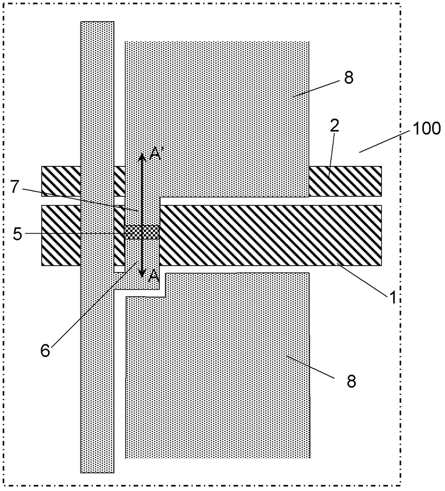
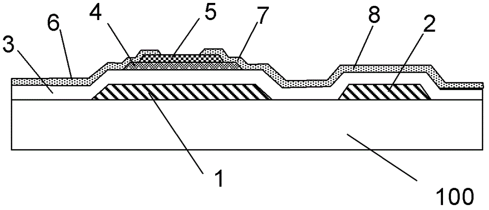
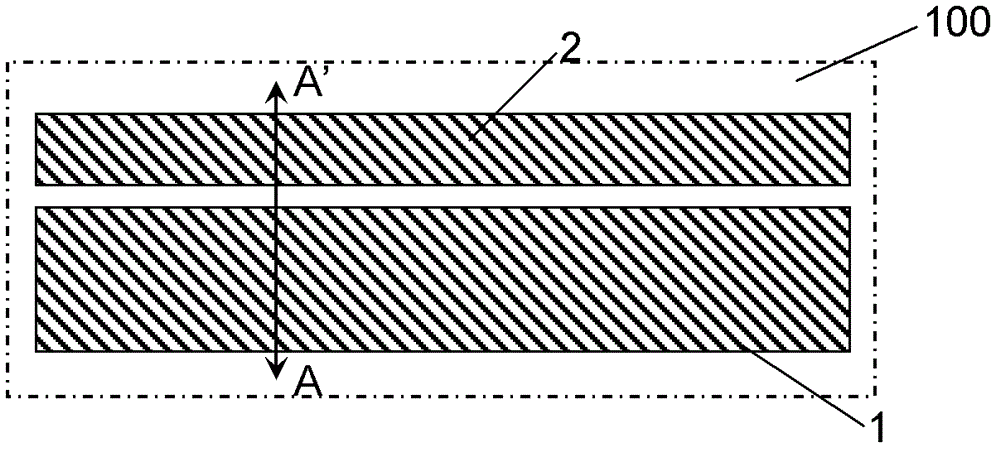
[0046] figure 1 A schematic diagram showing a pixel structure of a pixel region of the array substrate of this embodiment, figure 2 yes figure 1 A-A' cross section in . As shown in the figure, a thin film transistor and a pixel electrode are formed in a pixel area. Specifically, a gate 1 and a common electrode 2 are formed on the substrate 100, a gate insulating layer 3 is continuously covered above the gate 1 and the common electrode 2, and a semiconductor layer is...
Embodiment 2
[0050] The structure of the liquid crystal display array substrate of this embodiment is the same as that of the array substrate of Embodiment 1, the difference being that the source electrode 6 and the drain electrode 7 of this embodiment are also made of graphene. Because the source electrode 6, the drain electrode 7 and the pixel electrode 8 belong to the same level in the preparation process, and the drain electrode 7 and the pixel electrode 8 are conductively connected, the preparation of the source electrode 6, the drain electrode 7 and the pixel electrode 8 is made of graphene. The process is simpler and the cost is lower. The setting of the etching stopper layer 5 in this embodiment can protect the active layer 4 from corrosion damage caused by the preparation of the source electrode 6 , the drain electrode 7 and the pixel electrode 8 .
Embodiment 3
[0052] The structure of the liquid crystal display array substrate of this embodiment is the same as that of the array substrate of Embodiment 1, the difference being that the source electrode 6 and the drain electrode 7 of this embodiment are made of graphene. Because the source electrode 6 and the drain electrode 7 belong to the same level in the preparation process, the preparation process is simple, and the source electrode 6 and the drain electrode 7 made of graphene have high chemical stability, good flexibility, and are not prone to ion diffusion. Damage, applicable to a variety of substrates, such as flexible substrates.
PUM
 Abstract
Description
Claims
Application Information
 - R&D
- Intellectual Property
- Life Sciences
- Materials
- Tech Scout
- Unparalleled Data Quality
- Higher Quality Content
- 60% Fewer Hallucinations
Browse by: Latest US Patents, China's latest patents, Technical Efficacy Thesaurus, Application Domain, Technology Topic, Popular Technical Reports.
© 2025 PatSnap. All rights reserved.Legal|Privacy policy|Modern Slavery Act Transparency Statement|Sitemap|About US| Contact US: help@patsnap.com