Light-emitting diode (LED) substrate lift-off method
A substrate and light spot technology, which is applied in the field of LED substrate peeling off by femtosecond laser, can solve the problems of easily damaged gallium nitride epitaxial layer, high heat, and broken chemical bonds, etc., and achieve the effect of improving light extraction efficiency and production yield
- Summary
- Abstract
- Description
- Claims
- Application Information
AI Technical Summary
Problems solved by technology
Method used
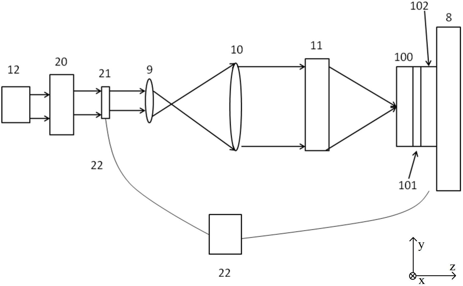
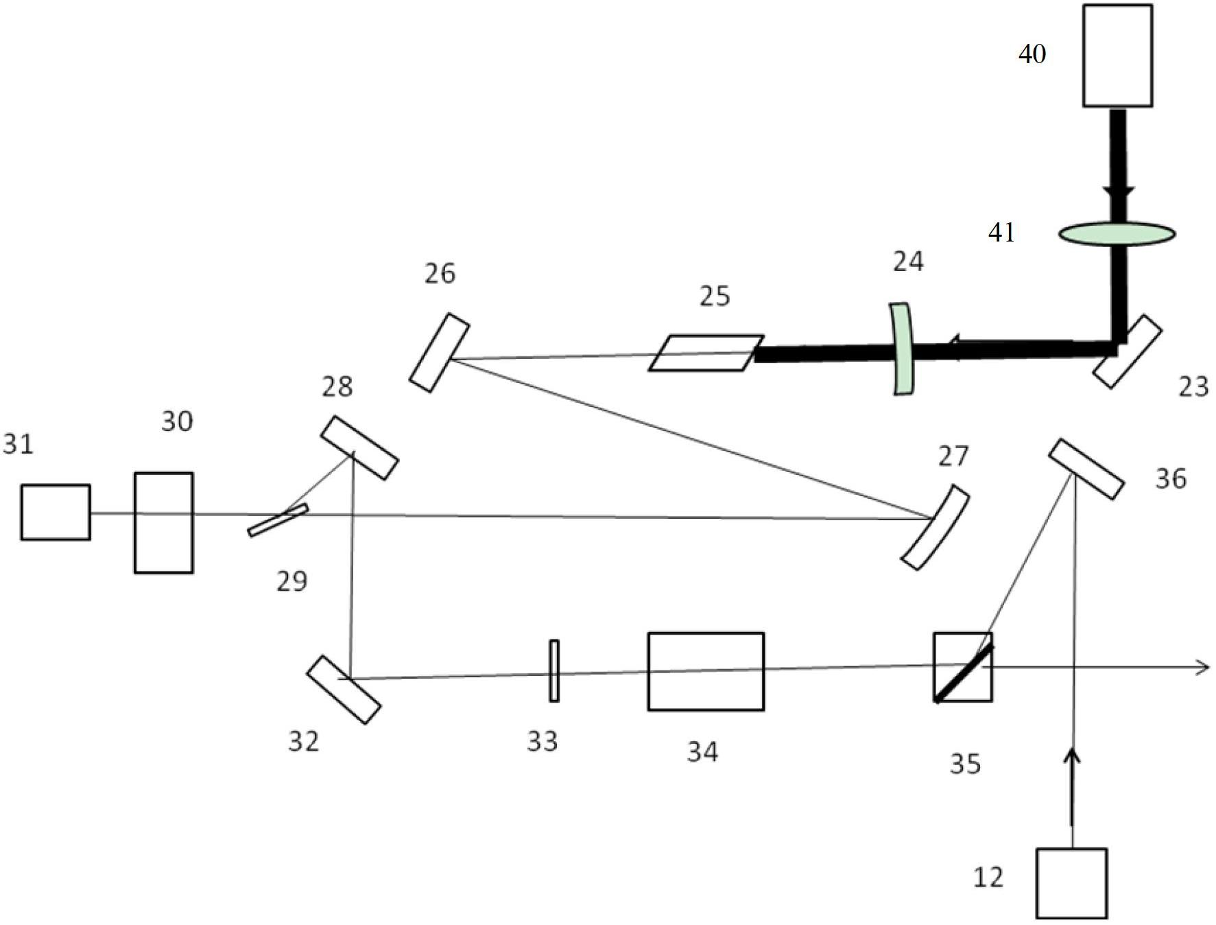
Image

Examples
Embodiment Construction
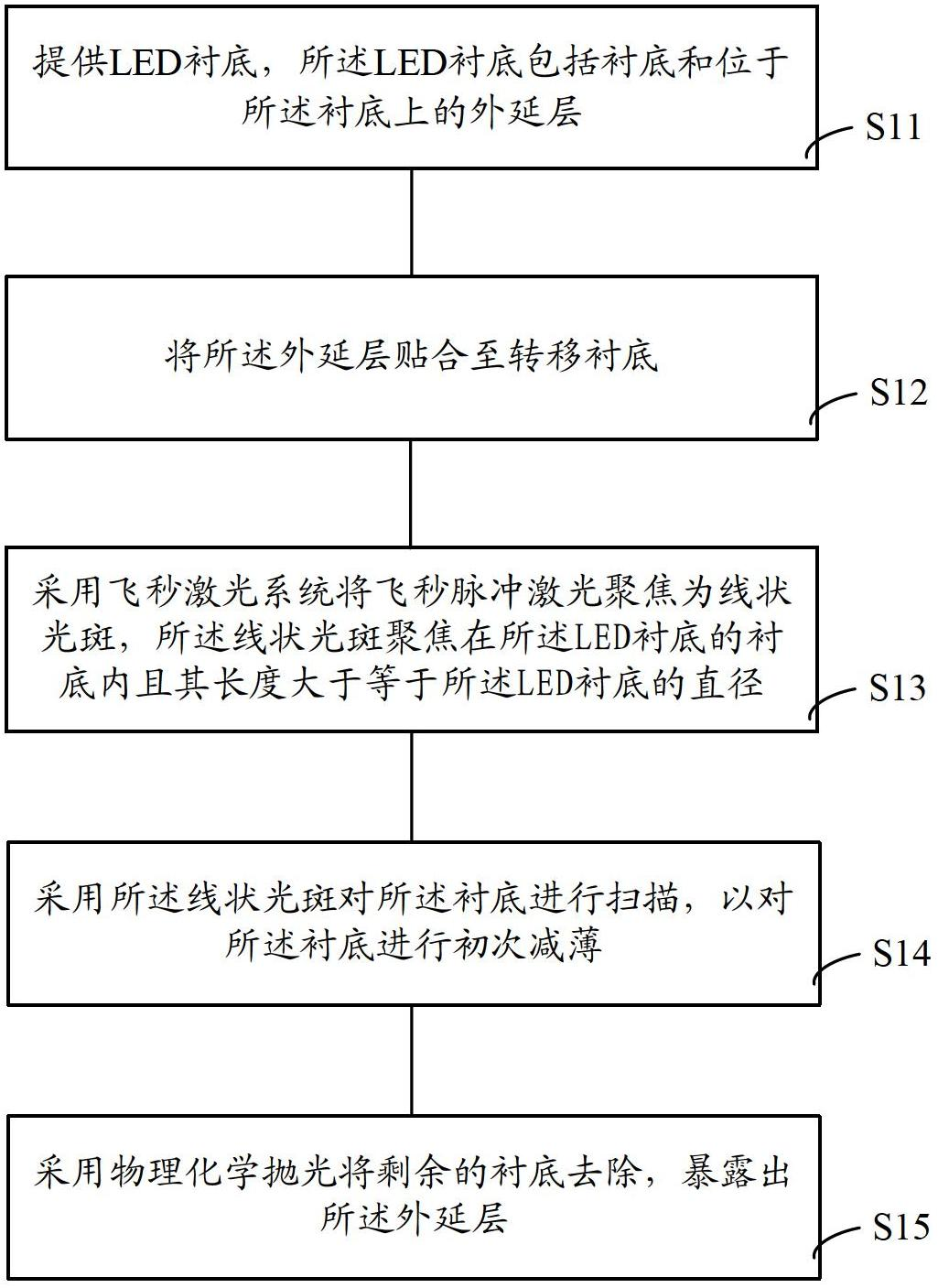
[0048] The present invention will be further described below in conjunction with specific embodiments and accompanying drawings, but the protection scope of the present invention should not be limited thereby.
[0049] figure 1 The process flow of the stripping method of the LED substrate of this embodiment is shown, including:
[0050] Step S11, providing an LED substrate, the LED substrate comprising a substrate and an epitaxial layer on the substrate;
[0051] Step S12, attaching the epitaxial layer to the transfer substrate;
[0052] Step S13, using a femtosecond laser system to focus the femtosecond pulse laser into a linear spot, the linear spot is focused in the substrate of the LED substrate and its length is greater than or equal to the diameter of the LED substrate;
[0053]Step S14, scanning the substrate by using the linear spot to thin the substrate for the first time;
[0054] In step S15, the remaining substrate is removed by physicochemical polishing to expo...
PUM
| Property | Measurement | Unit |
|---|---|---|
| thickness | aaaaa | aaaaa |
| diameter | aaaaa | aaaaa |
| diameter | aaaaa | aaaaa |
Abstract
Description
Claims
Application Information
 - R&D
- Intellectual Property
- Life Sciences
- Materials
- Tech Scout
- Unparalleled Data Quality
- Higher Quality Content
- 60% Fewer Hallucinations
Browse by: Latest US Patents, China's latest patents, Technical Efficacy Thesaurus, Application Domain, Technology Topic, Popular Technical Reports.
© 2025 PatSnap. All rights reserved.Legal|Privacy policy|Modern Slavery Act Transparency Statement|Sitemap|About US| Contact US: help@patsnap.com