Low-temperature polycrystalline silicon TFT (Thin Film Transistor) array substrate and manufacturing method thereof
A technology of low-temperature polysilicon and array substrates, applied in semiconductor/solid-state device manufacturing, optics, instruments, etc., can solve the problems of increased processing time and processing cost, complex manufacturing process, and various manufacturing processes, and achieve process reduction of exposure. Effect of reducing processing cost and shortening processing time
- Summary
- Abstract
- Description
- Claims
- Application Information
AI Technical Summary
Problems solved by technology
Method used
Image

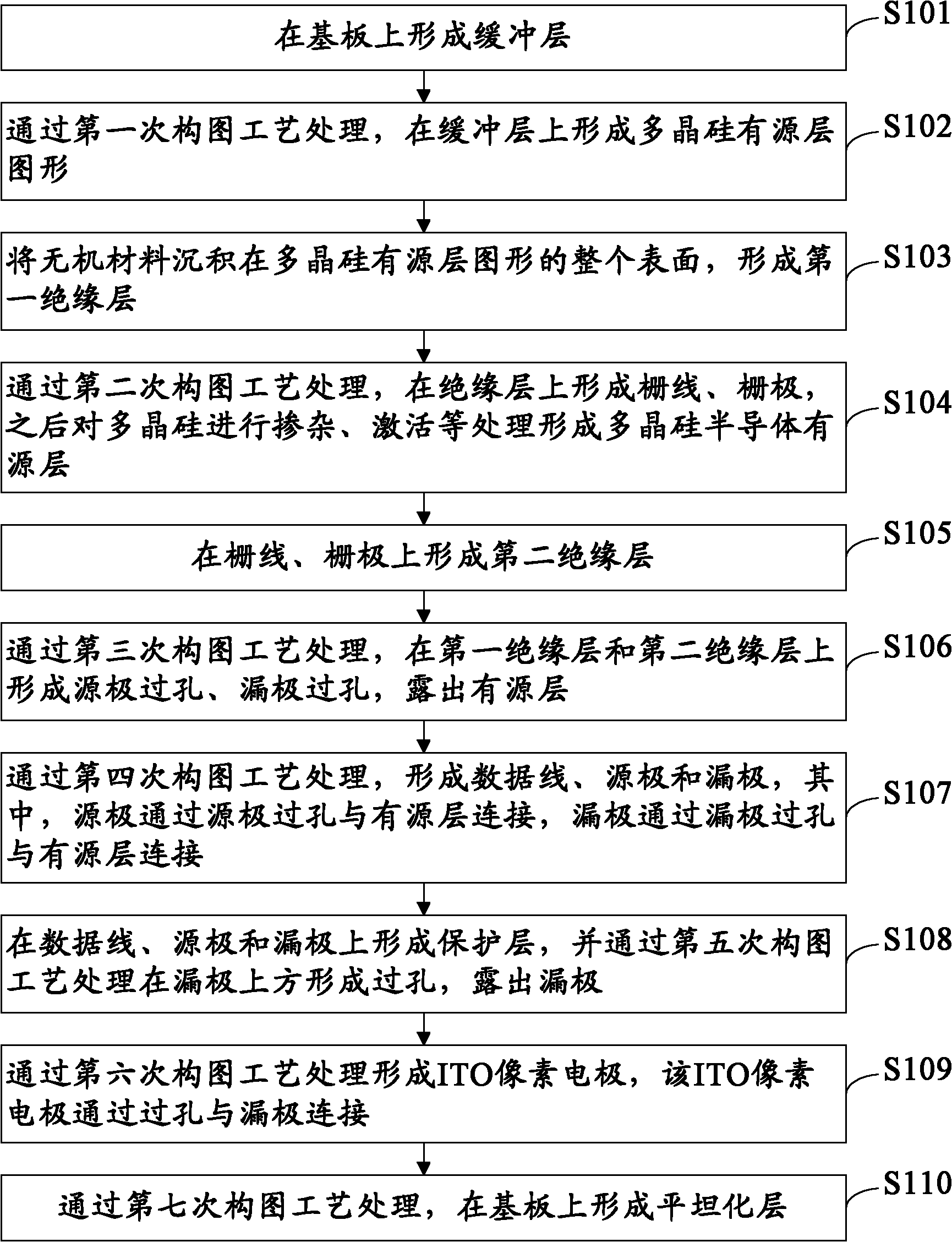
Examples
Embodiment 1
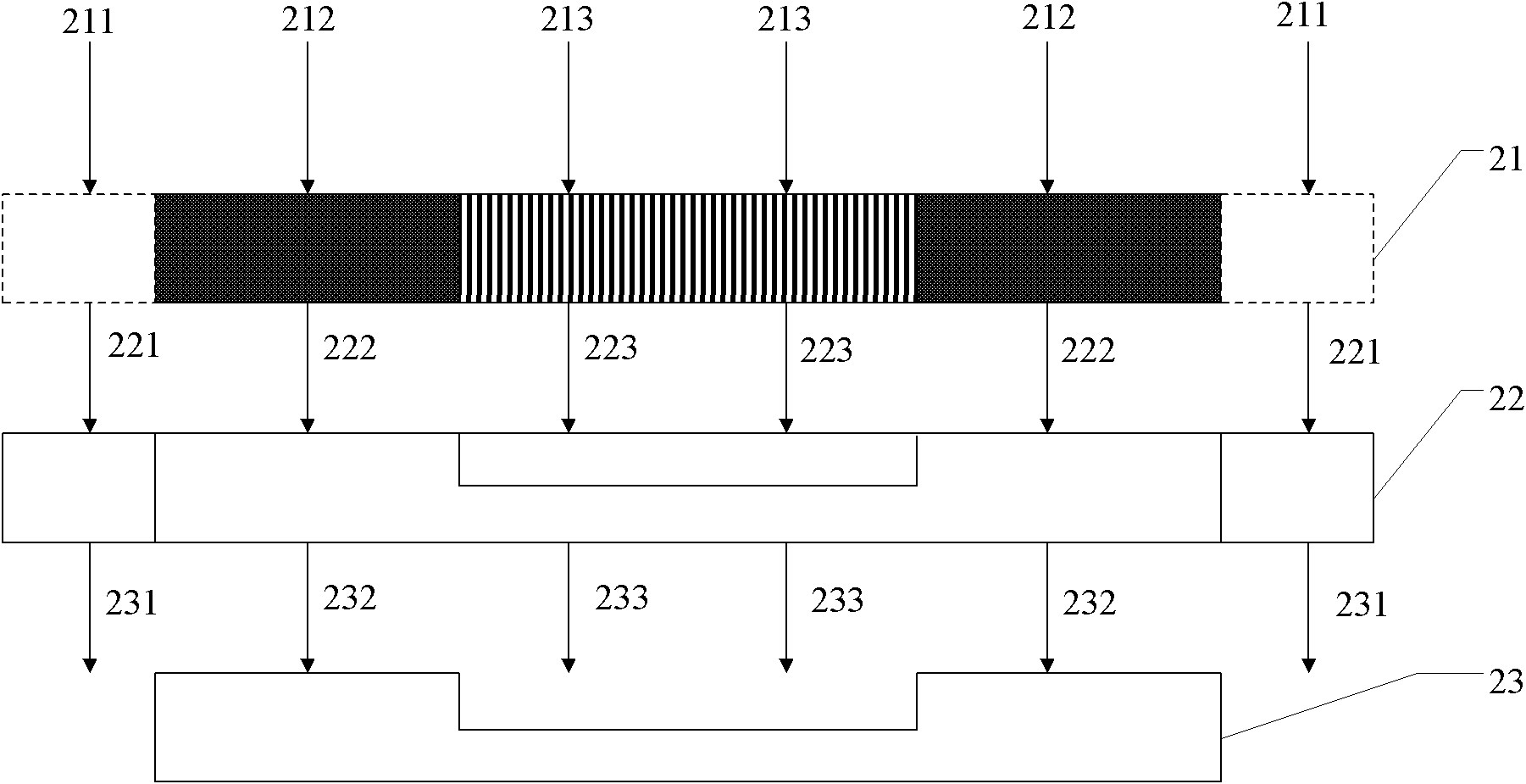
[0065] The method for manufacturing a low-temperature polysilicon TFT array substrate provided in Embodiment 1 of the present invention is described by taking the manufacture of a low-temperature polysilicon TFT array substrate by using a gray tone mask (GTM) as an example.
[0066] First, refer to Figure 3a The main principles of the GTM process are explained. The GTM mask plate uses the grating effect to make the intensity of the transmitted light different in different areas, so that the photoresist can be selectively exposed and developed. Figure 3a It shows the process of using the GTM mask 21 to expose the photoresist. In the GTM mask 21 , a transparent area 211 , an opaque area 212 and a translucent area 213 are included. The photoresist 22 is in a state after exposure, wherein the region 221 corresponds to the transparent region 211 of the GTM mask 21, the region 222 corresponds to the opaque region 212 of the GTM mask 21, and the region 223 corresponds to the tran...
Embodiment 2
[0097] The method for manufacturing a low-temperature polysilicon TFT array substrate provided in Embodiment 2 of the present invention is described by taking the manufacture of a low-temperature polysilicon TFT array substrate by using a semi-transparent mask (HTM) as an example.
[0098] First, refer to Figure 3b The main principle of the HTM process is explained. The HTM mask plate is used to selectively expose and develop the photoresist through the different intensity of light transmitted in different areas. Figure 3b It shows the process of exposing the photoresist by using the HTM mask 31 . In the HTM mask 31 , a transparent area 311 , an opaque area 312 and a translucent area 313 are included. The photoresist 32 is the state after exposure, wherein, the region 321 corresponds to the transparent region 311 of the HTM mask 31, the region 322 corresponds to the opaque region 312 of the HTM mask 31, and the region 323 corresponds to the translucent region of the HTM ma...
Embodiment 3
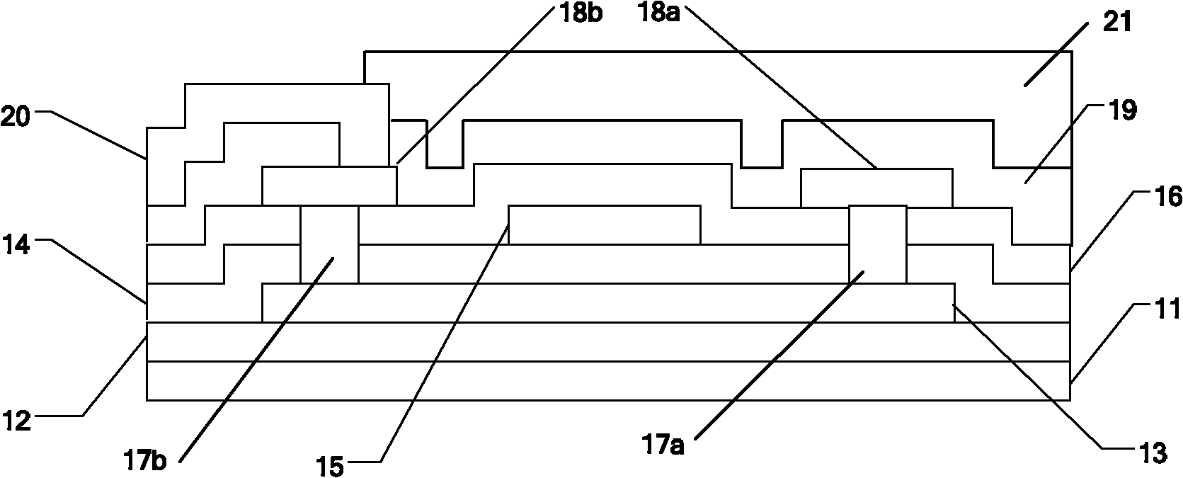
[0121] The low-temperature polysilicon TFT array substrate provided by the embodiment of the present invention, such as Figure 5Q shown, including:
[0122] Substrate 51;
[0123] A buffer layer 52 is formed on the substrate 51;
[0124] A polysilicon semiconductor active layer 53 is formed on the buffer layer 52;
[0125] A source 541 and a drain 542 are formed on the polysilicon semiconductor active layer 53; the source 541, the drain 542 and the polysilicon semiconductor active layer 53 form a TFT region;
[0126] A gate insulating layer 56 is formed on the source 541 and the drain 542;
[0127] A gate 57 and a gate line (not shown in the figure) are formed on the gate insulating layer 56;
[0128] A protective layer 58 is formed on the gate 57 and the gate line;
[0129] A pixel electrode layer 59 is formed on the protective layer 58, and the pixel electrode layer 59 is connected to the drain electrode 542 through a via hole 59' located on the protective layer 58 and...
PUM
 Abstract
Description
Claims
Application Information