Metal oxide thin film transistor with top gate structure and manufacturing method thereof

A technology of oxide thin film and oxide film layer, which is applied in the direction of transistors, semiconductor devices, electrical components, etc., can solve the problems of insufficient device characteristics, uniformity and stability, improve the annealing process and environment, and increase electron mobility , to reduce the effect of charge defects

Inactive Publication Date: 2012-09-19
东莞彩显有机发光科技有限公司 +2
View PDF4 Cites 16 Cited by
  • Summary
  • Abstract
  • Description
  • Claims
  • Application Information

AI Technical Summary

Problems solved by technology

[0007] The technical problem to be solved by the present invention is to provide a top-gate structure metal oxide thin film transistor with excellent stability and uniformity in view of the insufficient characteristics, uniformity and stability of existing thin film transistor devices; for this reason, the present invention also provides A method for manufacturing the top gate structure metal oxide thin film transistor

Method used


Image

  • Metal oxide thin film transistor with top gate structure and manufacturing method thereof
  • Metal oxide thin film transistor with top gate structure and manufacturing method thereof
  • Metal oxide thin film transistor with top gate structure and manufacturing method thereof

Examples


Embodiment 1

[0041] (1) Sputtering 20nm oxygen-deficient IGZO (made in a single-component Ar atmosphere) on the alkali-free glass, and then sputtering 5nm oxygen-enriched IGZO (made in a single-component oxygen atmosphere) with the same target; then wet etching Eclipse, graphical IGZO;

[0042] (2) Anneal in a dry oxygen atmosphere at 300°C for one hour;

[0043] (3) Sputtering 20nm silicon dioxide and 300nm silicon nitride on the composite active layer as the insulating layer;

[0044] (4) Anneal in air at 200°C for one hour;

[0045] (5) Sputtering 100nm metal molybdenum as the gate electrode;

[0046] (6) Sputtering 100nm metal molybdenum as source / drain electrodes.

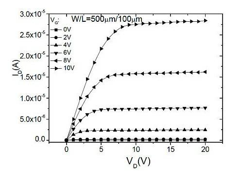
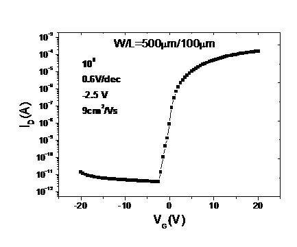
[0047] In addition, in this embodiment 1, please refer to the output characteristic curve figure 2 , please refer to the transfer characteristic curve image 3 .

Embodiment 2

[0049] In this implementation, a thin film transistor was fabricated according to a method and conditions similar to those of Example 1. The difference is that the following two steps are added between (5) and (6):

[0050] (6) Sputtering 5nm metal aluminum for metallizing the active layer;

[0051] (7) Anneal in a dry oxygen atmosphere at 300°C for one hour.

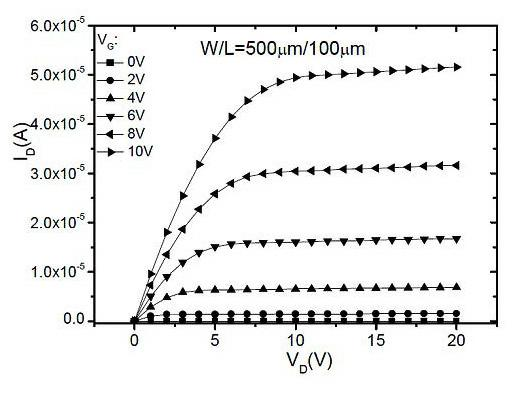
[0052] In addition, in this Example 2, please refer to the output characteristic curve Figure 4 , please refer to the transfer characteristic curve Figure 5 .

Embodiment 3

[0054] In this example, a thin film transistor was fabricated according to a method and conditions similar to those of Example 2. The difference is that the insulating layer annealing in step (4) is cancelled.


PUM


Abstract

The invention discloses a metal oxide thin film transistor with a top gate structure and a manufacturing method thereof. The thin film transistor comprises a substrate, an active layer, an insulating layer, a gate, a source and a drain, wherein the active layer is arranged on the substrate; the source is arranged at one end of the upper side of the active layer; the drain is arranged at the other end of the upper side of the active layer; the insulating layer is arranged in the middle of the upper side of the active layer; the gate is arranged on the insulating layer; a metallization layer is arranged between the active layer and the source; a metallization layer is also arranged between the active layer and the drain; and the active layer has a composite film structure and sequentially comprises an oxygen-poor metal oxide film layer and an oxygen-enriched metal oxide film layer from bottom to top. The active layer is made into the composite film layer through the same material and different processes, and the contact resistance in a source / drain electrode contact region is reduced through a metallization method; and the insulating layer is manufactured by employing an optimized sputtering process, and the plasma is prevented from damaging a channel active layer. Through the annealing treatment, the high-performance metal oxide thin film transistor with the top gate structure is obtained.

Description

technical field [0001] The invention relates to a thin film transistor, in particular to a metal oxide thin film transistor with a top gate structure and a manufacturing method thereof. Background technique [0002] Metal oxide thin film transistors are mainly used for organic light-emitting displays, liquid crystal displays, and active drives for electronic paper, and can also be used for integrated circuits. [0003] In recent years, thin film transistors based on metal oxides have attracted more and more attention because of their advantages such as high mobility, good light transmission, stable film structure, low fabrication temperature, and low cost. In particular, the oxide semiconductor TFT technology represented by In-Ga-Zn-O (IGZO) can achieve higher resolution compared to a-Si TFT, and can improve yield, reduce cost and reduce costs compared to LTPS TFT technology. Realize energy saving; Generally speaking, IGZO TFT technology has superior comprehensive performan...

Claims


Application Information

Patent Timeline
Patent Type & Authority Applications(China)
IPC IPC(8): H01L29/786H01L29/267H01L29/45
Inventor 张耿向桂华王娟赵伟明孙庆华蔡君蕊
Owner 东莞彩显有机发光科技有限公司
Why Eureka
Try Eureka