Low-temperature polycrystalline silicon thin film and production method thereof

A technology of low-temperature polysilicon and a manufacturing method, which is applied in semiconductor/solid-state device manufacturing, gaseous chemical plating, coating, etc., can solve the problems of uneven distribution and small grain size of polysilicon films, and achieve uniform distribution and grain size. The effect of large and low surface roughness

Active Publication Date: 2012-10-03
BOE TECH GRP CO LTD
View PDF2 Cites 32 Cited by
  • Summary
  • Abstract
  • Description
  • Claims
  • Application Information

AI Technical Summary

Problems solved by technology

At present, due to the inhomogeneity of polysilicon grains and the very large film roughness caused by the ordinary laser annealing process (in general

Method used


Image

  • Low-temperature polycrystalline silicon thin film and production method thereof
  • Low-temperature polycrystalline silicon thin film and production method thereof
  • Low-temperature polycrystalline silicon thin film and production method thereof

Examples


Example Embodiment

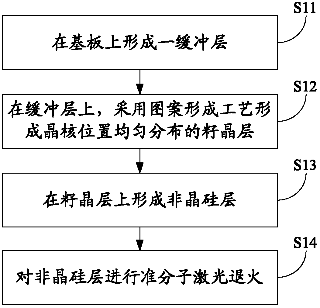
[0042] In order to make the technical problems, technical solutions and advantages to be solved by the embodiments of the present invention clearer, the following will describe in detail with reference to the drawings and specific embodiments.

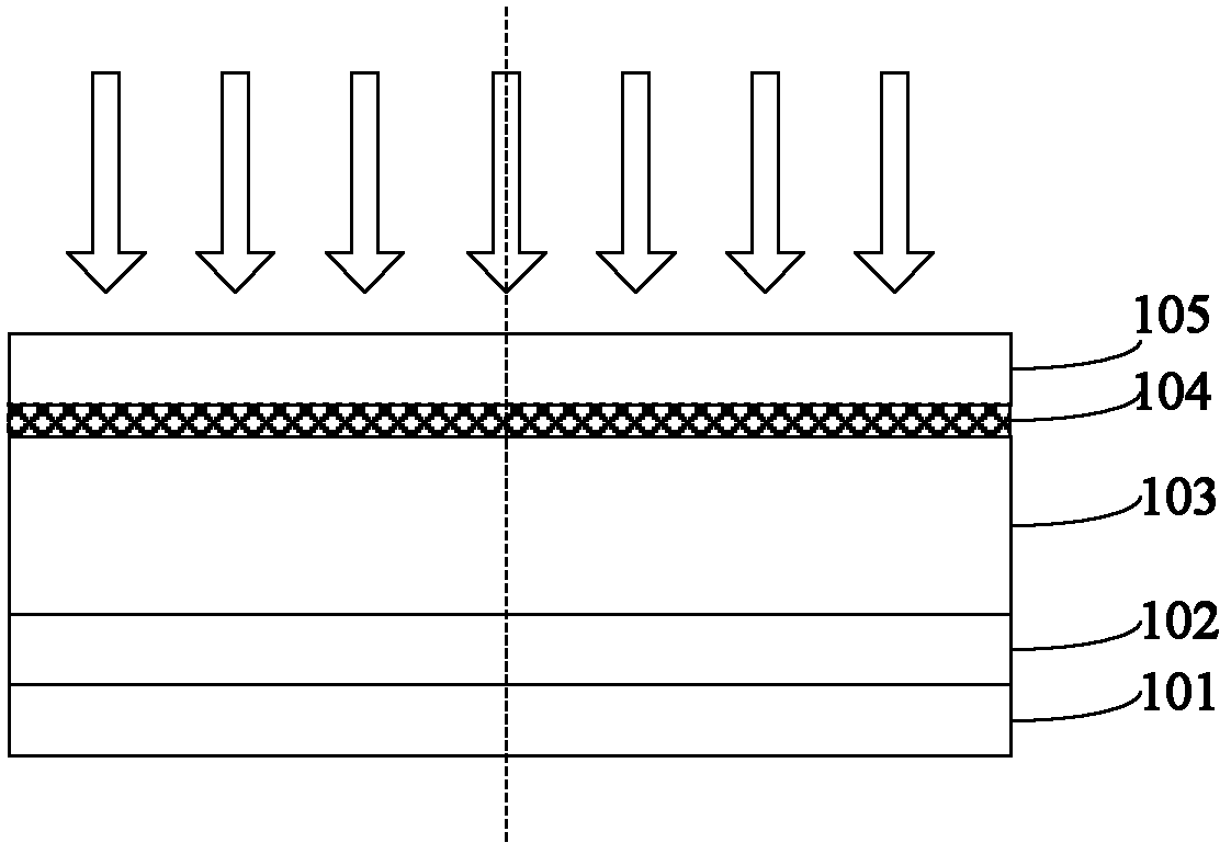
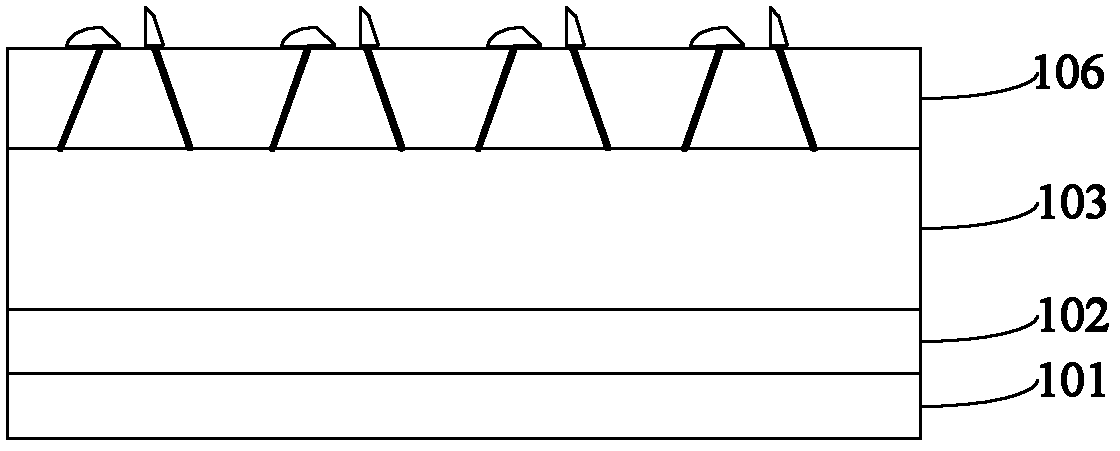
[0043] combine figure 1 and figure 2 As shown, the embodiment of the present invention provides a method for manufacturing a low-temperature polysilicon thin film, including the following steps S11-S14:

[0044] S11 , forming a buffer layer on the substrate 101 .

[0045] Among them, such as figure 2 shown, the buffer layer can be SiN x layer 102 with SiO 2 layer 103 composed of a composite buffer layer, at this time, the method for forming the composite buffer layer on the substrate 101 can be: on the substrate 101, first adopt PECVD (Plasma Enhanced Chemical Vapor Deposition, plasma enhanced chemical vapor deposition) method or Other deposition methods deposit a layer of SiN with a thickness of 50-150nm (the thickness can also...


PUM

PropertyMeasurementUnit
Thicknessaaaaaaaaaa

Abstract

The invention provides low-temperature polycrystalline silicon thin film and a production method thereof. The production method is used for producing low-temperature polycrystalline silicon thin film low in surface roughness, large in crystalline grain size and uniform in crystalline grain distribution and includes forming a buffer layer on a substrate, forming a seed crystal layer with crystal nucleus uniformly distributed on the buffer layer by means of the pattern forming technology; forming a non-crystalline-silicon layer on the seed crystal layer; and subjecting the non-crystalline-silicon layer to excimer laser annealing. The crystalline grains of the low-temperature polycrystalline silicon thin film produced by the production method are large in size and uniform in distribution, and further, the low-temperature polycrystalline silicon thin film is quite low in surface roughness, and accordingly solves the problems of low migration rate, high leakage current of thin-film transistors and unevenness of the migration rate and threshold voltage when being applied to a back plate of a low-temperature polycrystalline silicon display screen.

Description

technical field [0001] The invention relates to the technical field of low-temperature polysilicon thin films, in particular to a method for manufacturing a low-temperature polysilicon thin film and the low-temperature polysilicon thin film. Background technique [0002] With the advantages of high image quality, short response time of moving images, low power consumption, wide viewing angle and ultra-light and ultra-thin, AMOLED has become the best choice for future display technology. In the current AMOLED backplane technology, the technology for making polysilicon layer includes excimer laser annealing (ELA), solid phase crystallization (SPC), metal induced crystallization (MIC) and other manufacturing methods. However, using the excimer laser annealing (ELA) process to obtain the polysilicon thin film of the active layer of the transistor in the backplane is the only method that has achieved mass production. [0003] Excimer laser annealing process is a relatively compl...

Claims


Application Information

Patent Timeline
IPC IPC(8): H01L21/20H01L21/02H01L21/268
CPCH01L21/268H01L21/02532C23C16/0272C23C16/56H01L21/02488H01L21/02595C23C16/24H01L21/02686H01L21/32055H01L21/02502H01L21/0245H01L21/02505H01L21/02513H01L21/02516H01L21/02675
Inventor 田雪雁龙春平姚江峰
Owner BOE TECH GRP CO LTD
Why Eureka
Try Eureka