

Two-dimensional-three-dimensional mixed perovskite thin film and preparation and application thereof
A three-dimensional hybrid perovskite technology, applied in semiconductor/solid-state device manufacturing, semiconductor devices, electrical components, etc., can solve the problems of cumbersome and difficult-to-control stacked perovskite preparation methods, and achieve good photoelectric conversion efficiency and stability properties, low contact resistance, grain size and compactness
- Summary
- Abstract
- Description
- Claims
- Application Information
AI Technical Summary
Problems solved by technology
Method used
Image

Examples
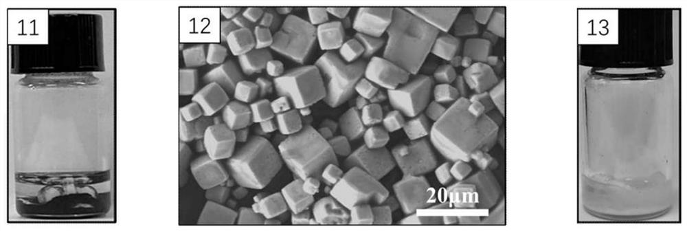
Embodiment 1
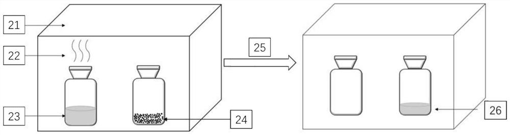
[0037] refer to figure 1 , 2 shown, including the following steps:
[0038] (1) PbI 2 and CH 3 NH 3 I joins in the aniline solvent according to molar ratio 1:1 (PbI 2 The concentration is 1M), stirred at 70°C for 12h to obtain solution A. Heat solution A to 100°C for about 2 to 3 hours, and small black crystals will precipitate out of the solution. Then suck out the excess solution, put the small black crystal grains and diethylamine in the same closed space, and let it stand for 6-12 hours to react, and the small black crystal grains will liquefy into a yellow liquid intermediate.
[0039] (2) PbI 2 and CH 3 NH 3 I joins in the DMF solvent according to molar ratio 1:1 (PbI 2 concentration is 1M), the solution was stirred at 70°C for 12h to obtain solution B; the yellow liquid intermediate obtained in step (1) was doped and added in different proportions (the volume ratio of the liquid intermediate was 5%, 10%, 20% , 30%, 60%) into solution B, and continued to stir ...
Embodiment 2
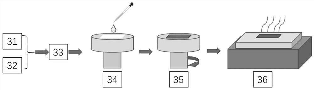
[0042] refer to image 3 As shown, the PCBM film was deposited on the perovskite film obtained in Example 1 with a spin-coating process of 1500 rpm and 30 s. last at 10 -4 A 100nm silver electrode was thermally evaporated at a vacuum degree of Pa.
PUM
| Property | Measurement | Unit |
|---|---|---|
| Size | aaaaa | aaaaa |
Abstract
Description
Claims
Application Information