Superfine crystal silicon battery structure

A crystalline silicon battery, ultra-thin technology, applied in circuits, electrical components, photovoltaic power generation, etc., can solve the problems of single optimization of photogenerated carrier generation, transportation and collection, to enhance the effect of light trapping in the body, and eliminate shading loss , Reduce the effect of recombination loss

Inactive Publication Date: 2014-07-02
BOHAI UNIV
View PDF5 Cites 0 Cited by
  • Summary
  • Abstract
  • Description
  • Claims
  • Application Information

AI Technical Summary

Problems solved by technology

[0006] The present invention aims to overcome the defects of single optimization of photogenerated carrier generation, transportation and collection processes in the existing battery efficiency technology, and provides a method that can optimize the optical and electrical efficiency synergies in the conversion process of the photoelectric cells inside the crystalline silicon battery. Ultra-thin crystalline silicon cell structure

Method used


Image

  • Superfine crystal silicon battery structure
  • Superfine crystal silicon battery structure
  • Superfine crystal silicon battery structure

Examples


Embodiment Construction

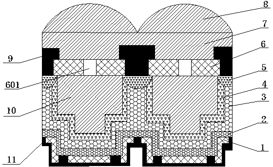
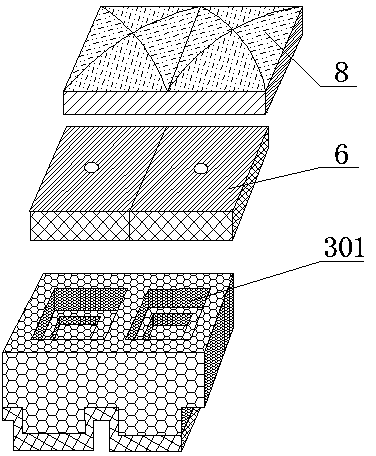
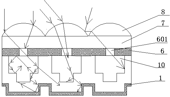
[0028] like figure 1 , figure 2 As shown, the ultra-thin crystalline silicon cell structure includes a P-type crystalline silicon wafer 3 with a stepped etching groove 301 on the front side, and an N-type doped region on the P-type crystalline silicon wafer 3 along the inner wall of the etching groove 301 4. A PN junction is formed through the N-type doped region 4, and a dielectric 10 is filled in the etching groove 301. The dielectric 10 is filled with polyimide (it can also be photoresist, magnesium fluoride, silicon dioxide, etc.) , aluminum oxide, silicon nitride, tantalum pentoxide, zinc sulfide or titanium dioxide), and a P+-type doped region 2 is provided on the back of the P-type crystalline silicon wafer 3 . An N+ doped region 5 is provided on the N-type doped region around the etching groove 301 on the front side of the silicon wafer 3, and an upper surface is provided on the upper surface of the dielectric 10 and the N-+ type doped region 5 on the front side of t...


PUM


Abstract

The invention provides a superfine crystal silicon battery structure which can realize the best synergism effect of an optical synergism structure and an electric synergism structure in a photovoltaic conversion process in a crystal silicon battery. The superfine crystal silicon battery structure comprises an upper surface medium reflection mirror, a P type crystal silicon sheet with a ladder-shaped etching groove on the front side and a lower surface medium reflection mirror, wherein the upper surface medium reflection mirror and the lower surface medium reflection mirror are respectively arranged on the front side and the back side of the P type crystal silicon sheet and form a quasi-three dimensional micro-cavity light trapping structure with the etching groove; a lighting hole is arranged in the center of the upper surface medium reflection mirror corresponding to the etching groove; the upper surface medium reflection mirror is provided with an optical buffering payer and a planoconvex lens; an N type doping region is arranged along the inner wall of the etching groove to form a PN junction with a P-type substrate; mediums are filled into the etching groove and a P-+ type doping region is arranged on the back surface of the crystal silicon sheet; an N+ doping region is arranged on the N- type doping region; a selective emission electrode is led out on the N+ doping region from the upper surface medium reflection mirror; and a backfield electrode is led out on the P-+ type doping region through the lower surface medium reflection mirror.

Description

technical field [0001] The invention relates to an ultra-thin crystalline silicon battery structure. Background technique [0002] Photovoltaic power generation is one of the main ways to utilize solar energy, but the high cost of photovoltaic power generation is still the main problem faced in this field. At present, crystalline silicon cells are in a monopoly position in the solar cell market, and they will still occupy an important position for a long time in the future. Therefore, greatly reducing the power generation cost of crystalline silicon cells is undoubtedly an important research in the field of photovoltaic power generation. subject. [0003] Ultra-thin crystalline silicon high-efficiency cell technology is the main way to solve the problem of power generation cost of crystalline silicon cells. According to the forecast of CTM (Crystalline Silicon PV Technology and Manufacturing Group): by 2020, the thickness of mass-produced crystalline silicon wafers will be...

Claims


Application Information

Patent Timeline
Patent Type & Authority Patents(China)
IPC IPC(8): H01L31/0232H01L31/0224H01L31/054
CPCY02E10/52
Inventor 陆晓东伦淑娴王巍郭艳东郭兆正于忠党周涛
Owner BOHAI UNIV
Why Eureka
Try Eureka