Production method for full back electrode solar cells
A technology for solar cells and production methods, which is applied in the manufacturing of circuits, electrical components, and final products, etc., can solve the problems of high cost and complicated battery preparation process steps, and achieve the effect of reducing production costs and improving battery efficiency.
- Summary
- Abstract
- Description
- Claims
- Application Information
AI Technical Summary
Problems solved by technology
Method used
Image
Examples
Embodiment Construction
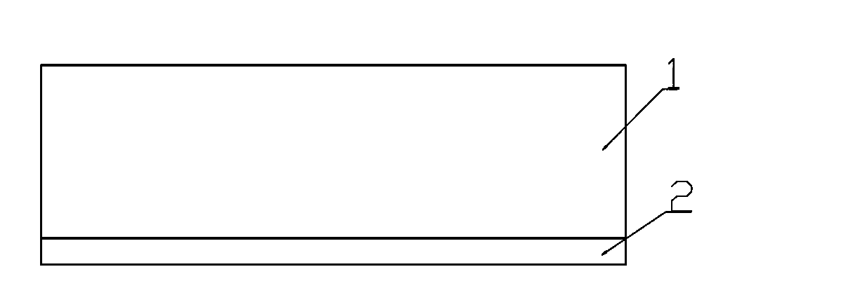
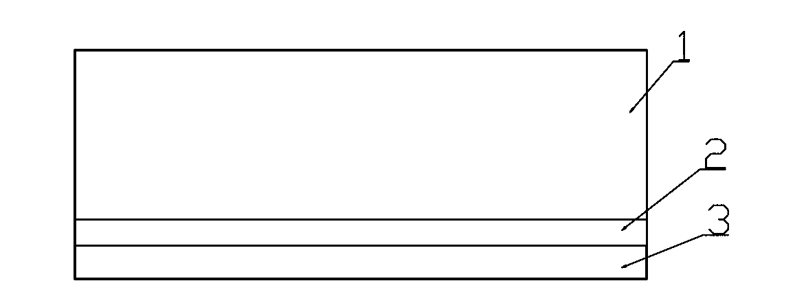
[0042] Such as Figures 1 to 14 Shown, a kind of production method of full back electrode solar cell has the following steps:
[0043] 1. Silicon wafer 1 is polished, and the etching thickness is 2-10um;
[0044] 2. Single-sided boron diffusion is performed on the silicon wafer 1 face to face, and a P+ layer 2 for forming a P-N junction is formed on the back of the silicon wafer 1, and the sheet resistance is 10-100ohm / Sq;
[0045] 3. Deposit SiNx or SiO2 or other texture mask layer 3 on the P+ layer 2 on the back side. The thickness of the texture mask layer 3 is 20-300nm, which can block the corrosion of the P+ layer 2 by the texture solution in the next step, and will not Destruction of the P-N junction;
[0046] 4. Single-sided texturing, the thickness of the texturing corrosion layer is 2-15um;
[0047] 5. The surface field before phosphorus diffusion preparation is 4, and the sheet resistance is 30-200ohm / Sq;
[0048] 6. Remove SiNx or SiO2 or other texture mask laye...
PUM
| Property | Measurement | Unit |
|---|---|---|
| Sheet resistance | aaaaa | aaaaa |
| Thickness | aaaaa | aaaaa |
| Sheet resistance | aaaaa | aaaaa |
Abstract
Description
Claims
Application Information


