In-wafer reliability screening method for GaN HEMT (High Electron Mobility Transistor) device

A reliability and device technology, applied in the direction of single semiconductor device testing, optical testing flaws/defects, etc., can solve the problems of reducing the electron gas concentration in the lower channel, device performance degradation, drain current and transconductance drop, etc., to achieve shortening The time of screening, the effect of improving work efficiency and improving reliability

Active Publication Date: 2012-10-10
NO 55 INST CHINA ELECTRONIC SCI & TECHNOLOGYGROUP CO LTD
View PDF6 Cites 12 Cited by
  • Summary
  • Abstract
  • Description
  • Claims
  • Application Information

AI Technical Summary

Problems solved by technology

[0002] GaN HEMT devices have experienced nearly two decades of development, and the microwave performance of the device has been gradually improved and approached its theoretical limit. However, because it is mostly used in the microwave high-power field, the device often works at a very high drain-source bias voltage. The hot electrons generated under high electric field will degrade the characteristics of HEMT devices, and the resulting reliability problems have hindered the development and wide application of G

Method used


Image

  • In-wafer reliability screening method for GaN HEMT (High Electron Mobility Transistor) device
  • In-wafer reliability screening method for GaN HEMT (High Electron Mobility Transistor) device

Examples


Embodiment 1

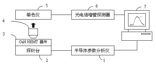
[0025] According to step 1 in the above-mentioned embodiment, a GaN HEMT device on-chip electroluminescence spectrum test platform is built.

[0026] GaN HEMT device on-chip electroluminescence calibration: turn off all light sources in the test site, do not apply any bias voltage to the GaN HEMT device, use the microscopic spectrum test system to test its response spectrum to black body radiation, and record the data Intensity0-λ in the computer .

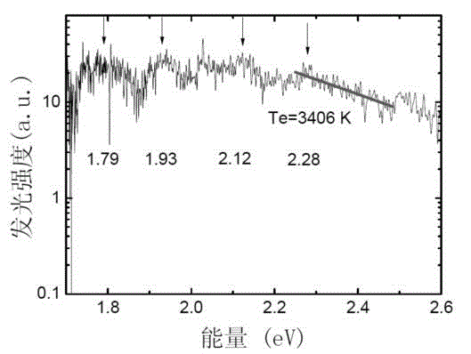
[0027] Selection of luminous intensity test conditions for GaN HEMT devices: First, test the transfer characteristics Ids-Vgs of the device to obtain the pinch-off voltage Vp=-1.76V of the device; then, make the gate voltage Vgs=-1.8V and gradually increase the drain voltage Vds At the same time, observe the device image in the computer. When the device starts to emit light, the leakage voltage is Vdsc=40V; select the leakage voltage Vds=35V test condition (the device does not emit light at this time), and measure the relationship...


PUM


Abstract

The invention discloses an in-wafer reliability screening method for a GaN HEMT (High Electron Mobility Transistor) device. The in-wafer reliability screening method is characterized by comprising the following steps that: firstly, in-wafer electroluminescence spectrum testing platform is established, a GaN heterojunction HEMT device wafer is placed on a probe platform in a darkroom, and then probes are respectively pressed on a grid electrode, a source electrode and a leakage electrode; and then, the source electrode is grounded, certain forward bias is applied to the leakage electrode, backward bias Vgs, which changes from pinch-off voltage Vp to 0V, is applied to the grid electrode, a change relationship between the luminous intensity of a GaN heterojunction HEMT device and grid voltage is tested by virtue of a spectrum testing system, the luminescence spectrum of the device is tested under the adopted bias point Vgsm with the largest luminous intensity, and then the spectrum is analyzed to evaluate the reliability of the device. The in-wafer reliability screening method has the advantages that in-wafer screening can be realized; a series of reliability screening preparation procedures, such as scribing and packaging, is eliminated without long-time electric stress; and the reliability screening time is shortened, costs are saved, and work efficiency is improved.

Description

technical field [0001] The invention relates to an on-chip screening method for the reliability of GaN HEMT devices, which is a method for screening the reliability of GaN HEMT devices by utilizing the GaN HEMT high-field luminescent phenomenon, and belongs to the technical field of semiconductor devices. Background technique [0002] GaN HEMT devices have experienced nearly two decades of development, and the microwave performance of the device has been gradually improved and approached its theoretical limit. However, because it is mostly used in the microwave high-power field, the device often works at a very high drain-source bias voltage. The hot electrons generated under high electric field will degrade the characteristics of HEMT devices, and the resulting reliability problems have always hindered the development and wide application of GaN HEMTs. Therefore, the study of GaN HEMT failure mechanism has always been a very important link in the field of GaN device researc...

Claims


Application Information

Patent Timeline
IPC IPC(8): G01R31/26G01N21/88
Inventor 孔月婵
Owner NO 55 INST CHINA ELECTRONIC SCI & TECHNOLOGYGROUP CO LTD
Why Eureka
Try Eureka