
Gd1-xCaxBiO3 buffering layer of high temperature superconducting coated conductor and preparation method thereof

A technology of coated conductors and high temperature superconductivity, which is applied in the directions of superconductivity/high conductivity conductors, the usage of superconductor elements, and cable/conductor manufacturing, etc. , to achieve the effect of low cost, suitable for large-scale deposition, and compact structure

Inactive Publication Date: 2012-10-10
SOUTHWEST JIAOTONG UNIV
View PDF4 Cites 3 Cited by
  • Summary
  • Abstract
  • Description
  • Claims
  • Application Information

AI Technical Summary

Problems solved by technology

However, most of these materials have a high melting point, and they need to be epitaxially grown at about 1000°C to form a buffer layer with good performance, and they need to be prepared under low oxygen partial pressure. The high preparation cost seriously affects the practical application of high-temperature coated conductors. progress

Method used


Image

  • Gd1-xCaxBiO3 buffering layer of high temperature superconducting coated conductor and preparation method thereof
  • Gd1-xCaxBiO3 buffering layer of high temperature superconducting coated conductor and preparation method thereof
  • Gd1-xCaxBiO3 buffering layer of high temperature superconducting coated conductor and preparation method thereof

Examples


Embodiment 1

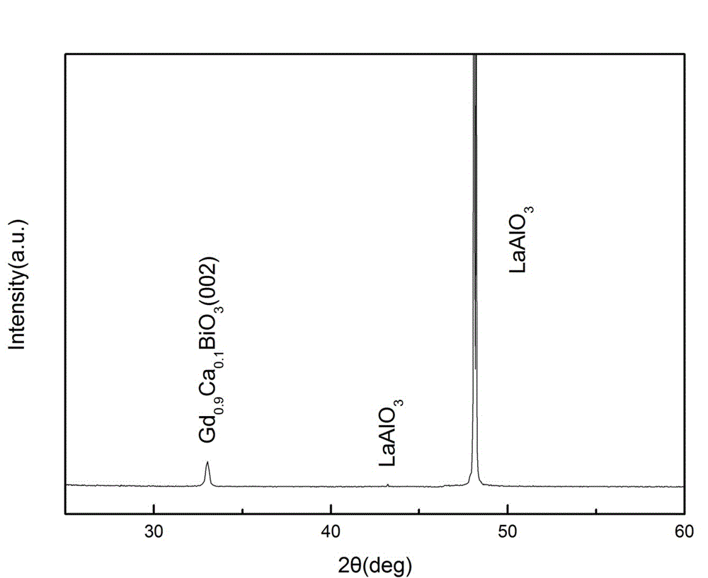
[0029] The invention provides a buffer layer Gd of a high-temperature superconducting coated conductor 0.9 Ca 0.1 BiO 3 . And a preparation of high temperature superconducting coating conductor Gd 0.9 Ca 0.1 BiO 3 The method for buffer layer thin film, its step is:

[0030] a.Gd 0.9 Ca 0.1 BiO 3 Preparation of buffer layer colloid: the precursors Gd, Ca, Bi nitrate are dissolved in an appropriate amount of polyacrylic acid (PAA) at a cationic concentration of 0.9:0.1:1 to obtain an organic system. The total molar concentration of the final solution is 0.2mol / L.

[0031] b.Gd 0.9 Ca 0.1 BiO 3 Buffer layer coating, drying and decomposition: coating the colloid prepared in step a on LaAlO 3 On the single crystal substrate, dry at 100°C; then place it in a sintering furnace, slowly raise the furnace temperature from room temperature to 180°C in the air, and raise it to 300°C at a speed of 0.1°C / min, and then Raise to 540°C at a rate of 0.1°C / min and keep warm for 30 ...

Embodiment 2

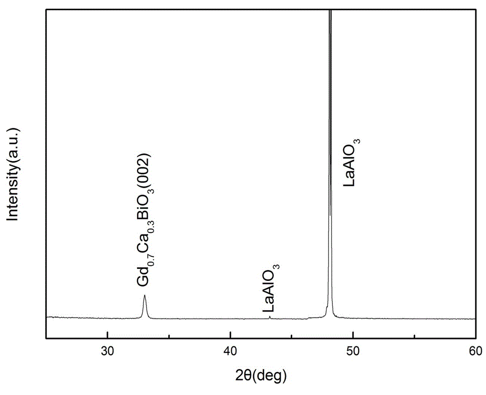
[0036] The invention provides a buffer layer Gd of a high-temperature superconducting coated conductor 0.7 Ca 0.3 BiO 3 . And a preparation of high temperature superconducting coating conductor Gd 0.7 Ca 0.3 BiO 3 The method for buffer layer thin film, its step is:

[0037] a.Gd 0.7 Ca 0.3 BiO 3 Preparation of buffer layer colloid: the precursor Gd, Ca, Bi nitrate is dissolved in an appropriate amount of polyacrylic acid (PAA) according to the cation concentration of 0.7:0.3:1, so as to obtain an organic system. The total molar concentration of the final solution is 0.2mol / L.

[0038] b.Gd 0.7 Ca 0.3 BiO 3 Buffer layer coating, drying and decomposition: coating the colloid prepared in step a on LaAlO 3 on a single crystal substrate, and then dried at 120°C; then placed in a sintering furnace, and the furnace temperature was slowly raised from room temperature to 200°C in the air, and then raised to 320°C at a speed of 2°C / min, and then Raise to 550°C at a rate of...

Embodiment 3

[0043] The invention provides a buffer layer Gd of a high-temperature superconducting coated conductor 0.6 Ca 0.4 BiO 3 . And a preparation of high temperature superconducting coating conductor Gd 0.6 Ca 0.4 BiO 3 The method for buffer layer thin film, its step is:

[0044] a.Gd 0.6 Ca 0.4 BiO 3 Preparation of buffer layer colloid: the precursors Gd, Ca, Bi nitrate are dissolved in an appropriate amount of polyacrylic acid (PAA) at a cation concentration of 0.6:0.4:1 to obtain an organic system. The total molar concentration of the final solution is 0.2mol / L.

[0045] b.Gd 0.6 Ca 0.4 BiO 3 Buffer layer coating, drying and decomposition: coating the colloid prepared in step a on LaAlO 3 On the single crystal substrate, dry at 150°C; then place it in a sintering furnace, slowly raise the furnace temperature from room temperature to 230°C in the air, and increase it to 340°C at a speed of 1°C / min, and then Raise to 560°C at a rate of 1°C / min and keep warm for 30 min...


PUM


Abstract

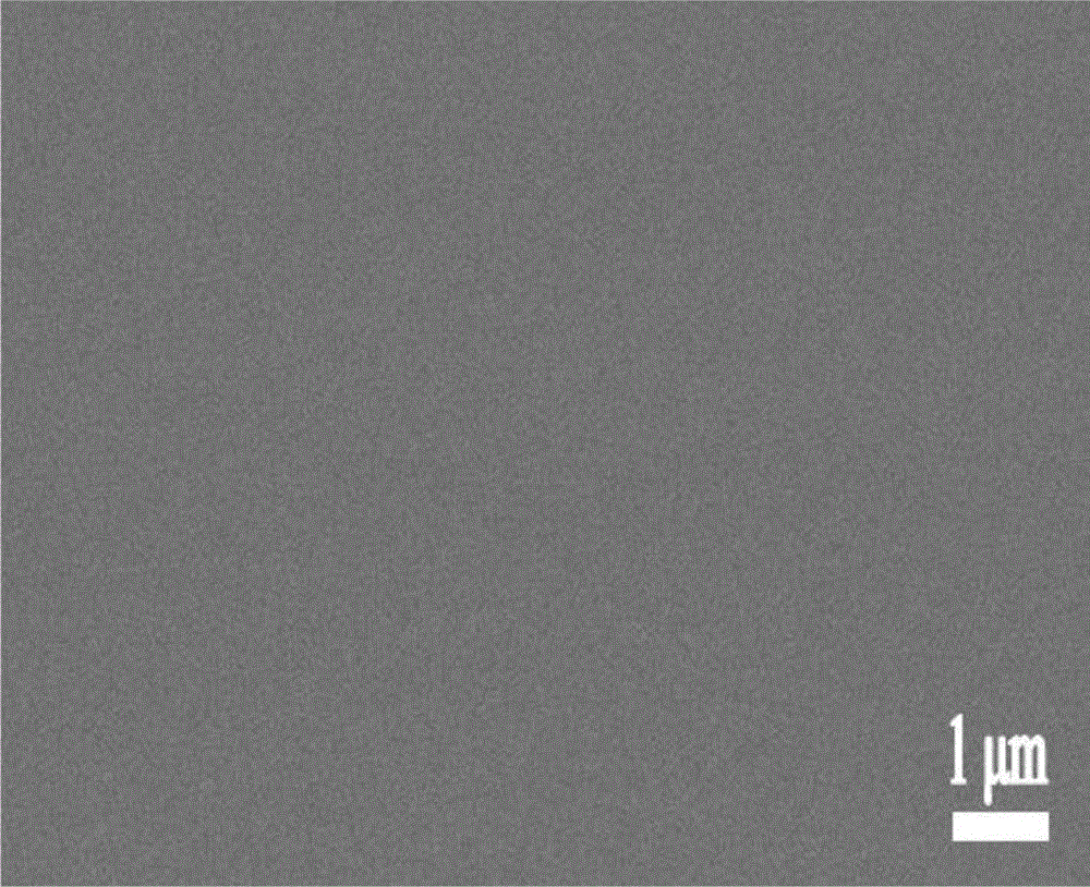
The invention discloses a Gd1-xCaxBiO3 buffering layer of a high temperature superconducting coated conductor. The buffering layer is characterized in that the Gd1-xCaxBiO3 buffering layer of the high temperature superconducting coated conductor epitaxially grows to generate an oxide Gd1-xCaxBiO3 solid solution through heat treatment after Gd in the Gd1-xCaxBiO3 buffering layer of the high temperature superconducting coated conductor is replaced with Ca, wherein x is not less than 0.1 and not more than 0.4. By using the Gd1-xCaxBiO3 buffering layer of the high temperature superconducting coated conductor disclosed by the invention, after Gd in the Gd1-xCaxBiO3 buffering layer of the high temperature superconducting coated conductor is replaced with Ca, an element environment and crystal lattice parameters of the GdBiO3 buffering layer are finely adjusted and then the lattice mismatch situation of the GdBiO3 buffering layer and a REBCO superconducting layer is adjusted; the buffering layer can epitaxially grow in the air at about 810 DEG C and has compact structure and smooth surface; and the structure of the buffering layer is kept stable in the follow-up preparing process of a superconducting layer of a high temperature superconducting coated conductor. The invention provides a preparation method of the Gd1-xCaxBiO3 buffering layer; in the method, the Gd1-xCaxBiO3 buffering layer is prepared in the air by using a chemical solution deposition method with nitrates as a precursor; therefore, the preparation method has the advantages of low cost, easiness in operation control, suitability for large-scale deposition and the like.

Description

technical field [0001] The invention relates to the technical field of preparation of high-temperature superconducting materials, in particular to a high-temperature superconducting coated conductor Gd 1-x Ca x BiO 3 Buffer layer and its preparation technology. Background technique [0002] In recent years, the second-generation high-temperature superconducting tape, that is, rare-earth barium-copper-oxide-coated conductors, has attracted worldwide attention due to its potential application prospects. Because the second-generation high-temperature superconducting tape has better current-carrying performance than the first-generation bismuth-based superconductor in the liquid nitrogen temperature zone and external magnetic field, it is used in superconducting cables, generators, motors, magnetic energy storage and magnetic resonance imaging. etc. have important applications. Starting from the technological innovation and long-term interests of their own electric energy, t...

Claims


Application Information

Patent Timeline
IPC IPC(8): H01B12/00H01B13/00
CPCY02E40/64Y02E40/60
Inventor 张欣赵勇程翠华张勇
Owner SOUTHWEST JIAOTONG UNIV
Learn More