Supercharge Your Innovation With Domain-Expert AI Agents!

Multi-layer metal ohmic contact system adopting silicon alloys and manufacturing method thereof

A technology of ohmic contact and multi-layer metal, which is applied in the manufacture of semiconductor/solid-state devices, electrical components, circuits, etc., can solve the problems of device performance degradation, reduce ohmic contact resistance, and the influence of crystal quality of epitaxial materials, etc., to achieve small contact resistance, Control repeatability, good repeatability effect

Inactive Publication Date: 2012-10-17
NO 55 INST CHINA ELECTRONIC SCI & TECHNOLOGYGROUP CO LTD
View PDF2 Cites 9 Cited by
  • Summary
  • Abstract
  • Description
  • Claims
  • Application Information

AI Technical Summary

Problems solved by technology

[0005] Ti / Al / Ti / Au, Ti / Al / Ni / Au, Ti / Al / Pt / Au, Ti / Al / Mo / Au and other multilayer metal ohmic contact systems can form smaller ohmic contacts with AlGaN / GaN HEMTs resistance, but its ohmic contact resistivity is usually 0.3-0.4Ω mm, one of the methods that can be used to further reduce the ohmic contact resistance is to implant Si into the source and drain regions to realize n + Doping, but the Si implantation doping can only be achieved through the high temperature annealing activation process of 1200-1300 °C. + Doping, the temperature of this high-temperature annealing is higher than the growth temperature of the epitaxial material used in AlGaN / GaN HEMT, which is likely to affect the crystal quality of the epitaxial material and cause the degradation of device performance

Method used


Image

  • Multi-layer metal ohmic contact system adopting silicon alloys and manufacturing method thereof
  • Multi-layer metal ohmic contact system adopting silicon alloys and manufacturing method thereof
  • Multi-layer metal ohmic contact system adopting silicon alloys and manufacturing method thereof

Examples


Embodiment 1

[0034] Embodiment 1, in conjunction with Fig. 2, Figure 5 ,

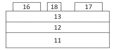
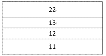
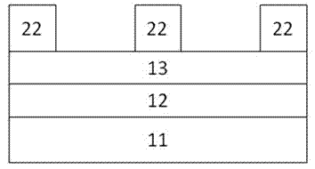
[0035] first as Figure 2A As shown, a photoresist layer 22 is coated on the AlGaN barrier layer 13, and then exposed and developed to form a Figure 2B The graph shown, again as Figure 2C The first ohmic contact metal layer 21 is shown on the AlGaN barrier layer 13 and the photoresist layer 22, and finally the photoresist layer 22 and the first ohmic contact metal layer 21 thereon are removed through stripping to obtain the following Figure 2D Source electrode 16 and drain electrode 17 are shown.

[0036] Wherein the first ohmic contact metal layer 21 such as Figure 5 As shown, it consists of four metal layers, starting from the interface between the AlGaN layer 13 and the first ohmic contact metal layer 21, the first TiSi alloy metal layer 51, the Al metal layer 52, the first barrier metal layer 53 and the first Au The metal layer 54 is composed. The thickness of the first TiSi alloy metal layer 51 is 15...

Embodiment 2

[0039] Embodiment 2, contrast image 3 , combined with Figure 2, Image 6 ,

[0040] first as Figure 2A As shown, a photoresist layer 22 is coated on the AlGaN barrier layer 13, and then exposed and developed to form a Figure 2B The graph shown, again as image 3 The second ohmic contact metal layer 31 is shown on the AlGaN barrier layer 13 and the photoresist layer 22, and finally the photoresist layer 22 and the second ohmic contact metal layer 31 thereon are removed through stripping to obtain the following Figure 2D Source electrode 16 and drain electrode 17 are shown.

[0041] The second ohmic contact metal layer 31 such as Image 6 As shown, it consists of four metal layers, starting from the interface of the AlGaN layer 13 and the second ohmic contact metal layer 31, sequentially consisting of a Ti metal layer 61, a first AlSi alloy metal layer 62, a second barrier metal layer 63 and a second Au metal layer. Metal layer 64, wherein the thickness of Ti metal lay...

Embodiment 3

[0044] Example 3, contrast Figure 4 , combined with Figure 2, Figure 7 ,

[0045] first as Figure 2A As shown, a photoresist layer 22 is coated on the AlGaN barrier layer 13, and then exposed and developed to form a Figure 2B The graph shown, again as Figure 4 The third ohmic contact metal layer 41 shown is on the AlGaN barrier layer 13 and the photoresist layer 22, and finally the photoresist layer 22 and the third ohmic contact metal layer 41 thereon are removed through stripping to obtain the following Figure 2D Source electrode 16 and drain electrode 17 are shown.

[0046] Wherein the third ohmic contact metal layer 41 such as Figure 7 As shown, it consists of four metal layers, starting from the interface of the AlGaN layer 13 and the third ohmic contact metal layer 41, the second TiSi alloy metal layer 71, the second AlSi alloy metal layer 72, the third barrier metal layer 73 and The third Au metal layer 74 is composed. The thickness of the second TiSi allo...


PUM

PropertyMeasurementUnit
thicknessaaaaaaaaaa
thicknessaaaaaaaaaa
thicknessaaaaaaaaaa

Abstract

The invention relates to a multi-layer metal ohmic contact system adopting silicon alloys and a manufacturing method thereof. The ohmic contact of a source electrode 16 and an drain electrode 17 has a structure of AlGaN / GaNHEMT, and adopts a TiSi / Al / Ni / Au or Ti / AlSi / Ni / Au or TiSi / AlSi / Ni / Au multi-layer metal system, wherein the TiSi and AlSi alloys are deposited by double-source electron beam evaporation or sputtering; and Al, Ni and Au are deposited by electron beam evaporation or sputtering. The invention has the following advantages: the manufactured ohmic contact has less contact resistance and can well control the repeatability of the process.

Description

technical field [0001] The invention relates to a multilayer metal ohmic contact system using a silicon alloy and a manufacturing method thereof. It belongs to the field of semiconductor technology. Background technique [0002] Aluminum Gallium Nitride (AlGaN) / Gallium Nitride (GaN) High Electron Mobility Transistor (HEMT) third-generation wide-bandgap compound semiconductor devices have the characteristics of high output power and high operating frequency, and are suitable for high-power applications in millimeter wave and below frequency bands. This makes it a hot spot in the research of semiconductor microwave power devices in recent years. [0003] Ohmic contact is a key process in the development of AlGaN / GaN HEMT devices. Achieving small ohmic contact resistance is a necessary condition for obtaining high-performance AlGaN / GaN HEMTs. This is because ohmic contact resistance in AlGaN / GaN HEMT devices is a series The existence of resistance, its value directly affects ...

Claims


Application Information

Patent Timeline
Patent Type & Authority Applications(China)
IPC IPC(8): H01L29/45H01L29/778H01L21/28H01L21/335
Inventor 任春江陈堂胜
Owner NO 55 INST CHINA ELECTRONIC SCI & TECHNOLOGYGROUP CO LTD
Features
  • R&D
  • Intellectual Property
  • Life Sciences
  • Materials
  • Tech Scout
  • Unparalleled Data Quality
  • Higher Quality Content
  • 60% Fewer Hallucinations
Learn More