Blue-ray fluorescent organic light emitting diode and manufacturing method thereof

A light-emitting diode and blue light technology, which is applied in semiconductor/solid-state device manufacturing, electrical components, electric solid-state devices, etc., can solve the problems of device operating voltage increase and power efficiency decrease

Inactive Publication Date: 2012-10-17
CHANGCHUN INST OF APPLIED CHEMISTRY - CHINESE ACAD OF SCI
View PDF6 Cites 22 Cited by
  • Summary
  • Abstract
  • Description
  • Claims
  • Application Information

AI Technical Summary

Problems solved by technology

[0007] The purpose of the present invention is to provide a blue fluorescent organic light-emitting diode to solve the problem that the carrier transport material used in the existing blue fluorescent organic light-emitting diode does not match with the blue fluorescent dye, so that the working voltage of the device increases and the power efficiency decreases. Organic light emitting diode and its preparation method

Method used


Image

  • Blue-ray fluorescent organic light emitting diode and manufacturing method thereof
  • Blue-ray fluorescent organic light emitting diode and manufacturing method thereof
  • Blue-ray fluorescent organic light emitting diode and manufacturing method thereof

Examples


preparation example Construction

[0042] The present invention also provides a preparation method of a blue-light fluorescent organic light-emitting diode, the steps are as follows:

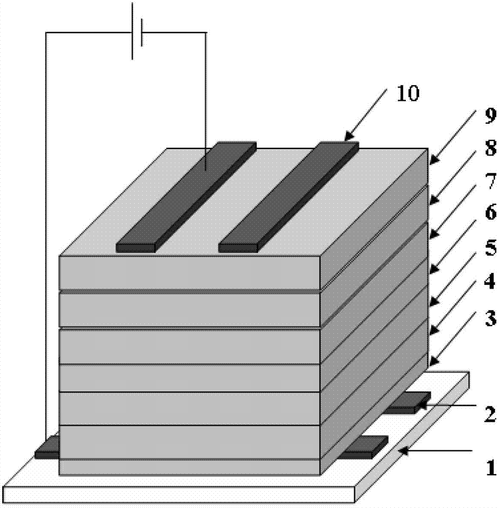
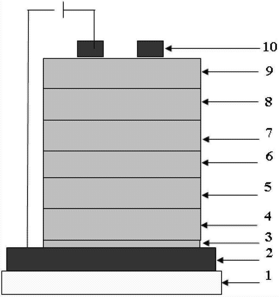
[0043] Carve the anode indium tin oxide into a thin strip electrode on a glass or flexible polymer substrate, then clean it, dry it with nitrogen, treat it with plasma for 1-5min, and bake it in a vacuum oven at 120°C for 30min-60min , and then transfer it to the vacuum coating system until the vacuum degree reaches 1 to 5×10 -4 At Pascal, the hole injection layer, the p-doped hole transport layer, the hole transport layer, the light-emitting layer, the electron transport / hole blocking layer, the n-doped electron transport layer, the electron injection layer and the cathode layer were evaporated in sequence, two of which The intersecting parts of the two electrodes form the light-emitting area of ​​the blue-light fluorescent organic light-emitting diode. The area of ​​the light-emitting area is 16 square millimeters. The thicknes...

Embodiment 1

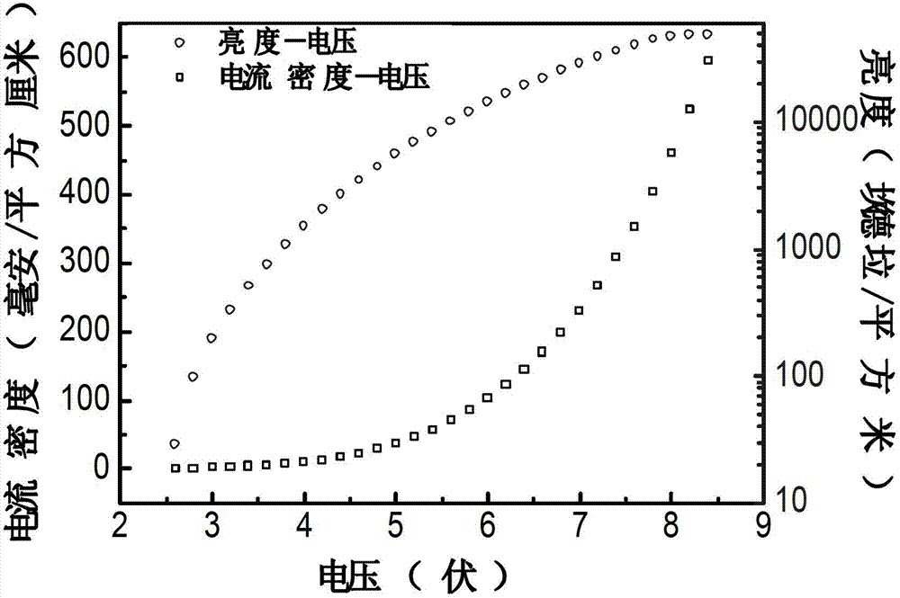
[0048] to combine figure 1 and figure 2 Illustrate present embodiment, first ITO on ITO glass 1 is photoetched into the electrode of 4 millimeters wide, 30 millimeters long, then described electrode is cleaned, nitrogen is blown dry and treated with oxygen plasma for 2 minutes, and in vacuum oven at 120 ℃ bake for 30min, and then transfer it to the vacuum coating system, until the vacuum degree reaches 1 to 5×10 -4 Pa, sequentially vapor-deposit M on the ITO electrode 2 O o 3 Hole injection layer 3, M O o 3 The hole transport layer 4 doped with NPB, the hole transport layer 5 of NPB, the light emitting layer 6 composed of BNE doped in the organic mixed host material composed of MADN and BANE, the electron transport / hole electron transport of Be(PP)2 Hole blocking layer 7, lithium carbonate doped Be (PP) Electron transport layer 8, lithium carbonate electron injection layer 9 and metal Al cathode 10, wherein two electrodes intersect with each other to form the light-emitt...

Embodiment 2

[0052] First, the ITO on the ITO glass is photolithographically formed into an electrode with a width of 4 mm and a length of 30 mm, then the electrode is cleaned, dried with nitrogen, treated with oxygen plasma for 2 minutes, and baked at 120 ° C for 30 minutes in a vacuum oven, and then Transfer it to a vacuum coating system until the vacuum reaches 1 to 5×10 -4 Pa, sequentially vapor-deposit V on the ITO electrode 2 o 5 hole injection layer, V 2 o 5 The hole transport layer doped with TCTA, the hole transport layer of TCTA, the light-emitting layer composed of pyrene doped in the organic mixed host material composed of MADN and BANE, the electron transport and hole blocking layer of Be(PP)2 , lithium carbonate-doped Be (PP) 2 electron transport layer, lithium carbonate electron injection layer and metal Al cathode, wherein two electrodes intersect with each other to form the light-emitting area of ​​the device, the area of ​​the light-emitting area is 16 square millimete...


PUM


Abstract

The invention provides a blue-ray fluorescent organic light emitting diode and a manufacturing method thereof, belongs to the technical field of organic semiconductors and solves the problems that the working voltage of a device is boosted, and the power efficiency is decreased because carrier transporting materials and blue-ray fluorescent dyes which are used in the conventional blue-ray fluorescent organic light emitting diode are not matched. The diode comprises a substrate, a first electrode, a light emitting unit and a second electrode, wherein the substrate, the first electrode, the light emitting unit and the second electrode are connected in sequence; the light emitting unit comprises a light emitting layer; and the light emitting layer consists of an organic mixture which is formed by doping the blue-ray fluorescent dyes with a mixed bipolar main body consisting of a hole-transporting blue-ray main material and an electron-transporting blue-ray main material. According to the blue-ray fluorescent organic light emitting diode, the turn-on voltage is 2.4V, the brightness is 1,000cd/m<2> when the voltage is 3.7V, the maximum current efficiency is 16.3cd/A, and the maximum power efficiency is 151m/W.

Description

technical field [0001] The invention belongs to the technical field of organic semiconductors, and in particular relates to a blue-light fluorescent organic light-emitting diode and a preparation method thereof. Background technique [0002] Organic light-emitting diode display is regarded as the most popular emerging display technology in the flat panel display industry, and has been extensively researched. Compared with inorganic light-emitting diodes, organic light-emitting diodes have a wide range of material selection, can realize full-color display from blue light area to red light area, low driving voltage, high luminous brightness and luminous efficiency, wide viewing angle, fast response speed, and manufacturing process. It has many advantages such as simplicity, low cost, and easy realization of large area and flexible display, so it has developed rapidly in the past 10 years. At present, the research on organic light-emitting diodes has long been limited to acade...

Claims


Application Information

Patent Timeline
Patent Type & Authority Applications(China)
IPC IPC(8): H01L51/54H01L51/50H01L51/56
Inventor 马东阁张智强刘一鹏代岩峰陈江山王艳平
Owner CHANGCHUN INST OF APPLIED CHEMISTRY - CHINESE ACAD OF SCI
Why Eureka
Try Eureka