Triazine compound and organic light-emitting device comprising same

A technology of organic light-emitting devices and compounds, applied in the field of organic electroluminescence, which can solve problems such as device performance degradation

Pending Publication Date: 2019-10-08
ZHEJIANG HUADISPLAY OPTOELECTRONICS CO LTD
View PDF7 Cites 3 Cited by
  • Summary
  • Abstract
  • Description
  • Claims
  • Application Information

AI Technical Summary

Problems solved by technology

[0004] The hole mobility of the hole transport material in the device is generally much greater than the elec

Method used


Image

  • Triazine compound and organic light-emitting device comprising same
  • Triazine compound and organic light-emitting device comprising same
  • Triazine compound and organic light-emitting device comprising same

Examples


Embodiment 1

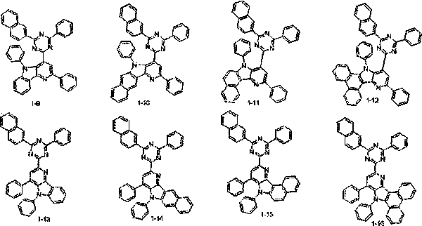
[0082] Synthesis of compound 1-1

[0083] (1) Synthesis of intermediate 1-1-1

[0084]

[0085] Add 2-(3-bromo-5-chlorophenyl)-4,6-diphenyl-1,3,5-triazine (0.8g, 1.18mmol), phenylboronic acid (0.2g, 1.66mmol), THF (30mL), potassium carbonate (2mol / L, 20mL), tetrakistriphenylphosphine palladium (100mg), and heated under reflux under nitrogen to react overnight. Stop the reaction, remove THF, extract three times with dichloromethane, combine the organic phases, wash with water until neutral, separate the organic phases, add anhydrous magnesium sulfate to dry, suction filter, spin dry; use silica gel column chromatography to obtain solid (0.41 g, yield 83%). LC-MS: M / Z 420.11 (M+H)+.

[0086] (2) Synthesis of Intermediate 1-1-2

[0087]

[0088] Add 2-(3-chloro-5-(pyridin-4-yl))-4,6-diphenyl-1,3,5-triazine (0.41g, 0.98mmol), 10- Nitrophenanthrene-9-boronic acid (0.25g, 1.47mmol), THF (40mL), potassium carbonate (2mol / L, 20mL), tetrakistriphenylphosphine palladium (100m...

Embodiment 2

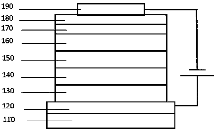
[0101] The transparent anode electrode ITO substrate was ultrasonically cleaned in isopropanol for 15 min and exposed to UV light for 30 min, followed by plasma treatment for 10 min. Then put the processed ITO substrate into the evaporation equipment. First evaporate a layer of 60nm NPB-DPA as the hole injection layer, the evaporation rate is 0.1nm / s, then evaporate 20nm NPB as the hole transport layer, the evaporation rate is 0.1nm / s, and then the light emitting layer The evaporation of mixed evaporation ADN / DPAVBi, the doping concentration is 2wt%, the evaporation rate of the matrix material is 0.1nm / s, the evaporation rate of the dopant material is 0.002nm / s, the evaporation thickness is 35nm, and then the evaporation Compound 1-1 was plated at 30nm as the electron transport layer at an evaporation rate of 0.05nm / s, and LiF and Al were vacuum-evaporated sequentially on the electron transport layer as the cathode with a thickness of 200nm.

Embodiment 3

[0103] The transparent anode electrode ITO substrate was ultrasonically cleaned in isopropanol for 15 min and exposed to UV light for 30 min, followed by plasma treatment for 10 min. Then put the processed ITO substrate into the evaporation equipment. First evaporate a layer of 60nm NPB-DPA as the hole injection layer, the evaporation rate is 0.1nm / s, then evaporate 20nm NPB as the hole transport layer, the evaporation rate is 0.1nm / s, and then the light emitting layer The evaporation of mixed evaporation ADN / DPAVBi, the doping concentration is 2wt%, the evaporation rate of the matrix material is 0.1nm / s, the evaporation rate of the dopant material is 0.002nm / s, the evaporation thickness is 35nm, and then the evaporation Plating 30nm of ET-1 as the electron transport layer, the evaporation rate is 0.05nm / s, and then 10nm of compound 1-1 as the hole blocking layer, and then vacuum-evaporating LiF and Al on the hole blocking layer as the cathode , with a thickness of 200nm.

...


PUM


Abstract

The invention relates to the technical field of organic electroluminescence and discloses a triazine compound and an organic light-emitting device comprising the same. On the one hand, a triazine group is stable in structure, high in glass transition temperature and electron mobility and low energy level, by bonding of the triazine group with a carbazole group especially through a benzene ring ora biphenyl ring, a conjugated system is increased, and a continuous pi conjugated system brings high electron mobility, so that high electron migration rate is achieved. In addition, due to bonding ofthe triazine group with the carbazole group, carrier transport balance is realized. By application of the triazine compound to the organic light-emitting device to serve as an electron transport layer or a hole barrier layer, and the device has advantages of low driving voltage and high light emitting efficiency and is superior to existing common OLED devices.

Description

technical field [0001] The invention relates to the technical field of organic electroluminescence, in particular to a triazine compound and an organic electroluminescence device using the compound. Background technique [0002] Organic Light Emitting Diode (OLED) is a light-emitting device prepared by using electrons and holes to recombine light in organic thin films. It has the following advantages: (1) Self-luminescence, no backlight is required; (2) Brightness High, with high contrast, pure color, almost no problem of viewing angle; (3) ultra-thin, composed of very thin organic material coating and matrix material, small size suitable for portable products; (4) power consumption Very small, environmentally friendly and energy-saving; (5) Fast response speed, one-thousandth of that of LCD; (6) Wide operating temperature range, and can still display normally at -40°C. [0003] Organic charge transport materials are a class of organic semiconductor materials that can achie...

Claims


Application Information

Patent Timeline
IPC IPC(8): C07D471/04C09K11/06H01L51/50H01L51/54
CPCC07D471/04C09K11/06C09K2211/1029C09K2211/1059C09K2211/1007C09K2211/1011C09K2211/1088C09K2211/1044H10K85/615H10K85/626H10K85/654H10K85/6572H10K85/6574H10K50/00H10K50/16
Inventor 高春吉黄东叶绪兵
Owner ZHEJIANG HUADISPLAY OPTOELECTRONICS CO LTD
Why Eureka
Try Eureka