
Strain SiGe square-in-square type channel NMOS (N-channel Metal Oxide Semiconductor) integrated device and preparation method thereof

An integrated device and channel direction technology, which is applied in semiconductor/solid-state device manufacturing, semiconductor devices, electrical components, etc. Devices and circuits, restricting the development of the semiconductor industry and other issues

Inactive Publication Date: 2015-07-22
XIDIAN UNIV
View PDF3 Cites 0 Cited by
  • Summary
  • Abstract
  • Description
  • Claims
  • Application Information

AI Technical Summary

Problems solved by technology

However, as the characteristic linewidth of silicon integrated circuits enters the nanometer scale, SiO 2 Traditional materials such as gate dielectric materials, polysilicon, and silicide gate electrodes have been unable to meet the needs of nanoscale devices and circuits due to the constraints of material characteristics. Requirements, therefore, silicon microelectronics technology is facing severe challenges, this situation seriously restricts the development of the semiconductor industry

Method used

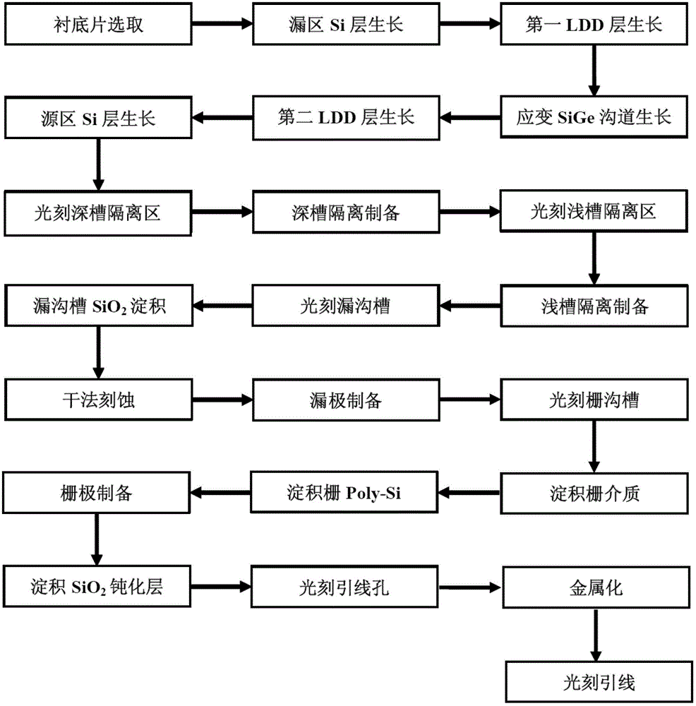

Image

  • Strain SiGe square-in-square type channel NMOS (N-channel Metal Oxide Semiconductor) integrated device and preparation method thereof
  • Strain SiGe square-in-square type channel NMOS (N-channel Metal Oxide Semiconductor) integrated device and preparation method thereof
  • Strain SiGe square-in-square type channel NMOS (N-channel Metal Oxide Semiconductor) integrated device and preparation method thereof

Examples


Embodiment 1

[0075] Embodiment 1: the preparation of the strained SiGe back channel NMOS integrated device and circuit with a conductive channel of 45nm, the specific steps are as follows:

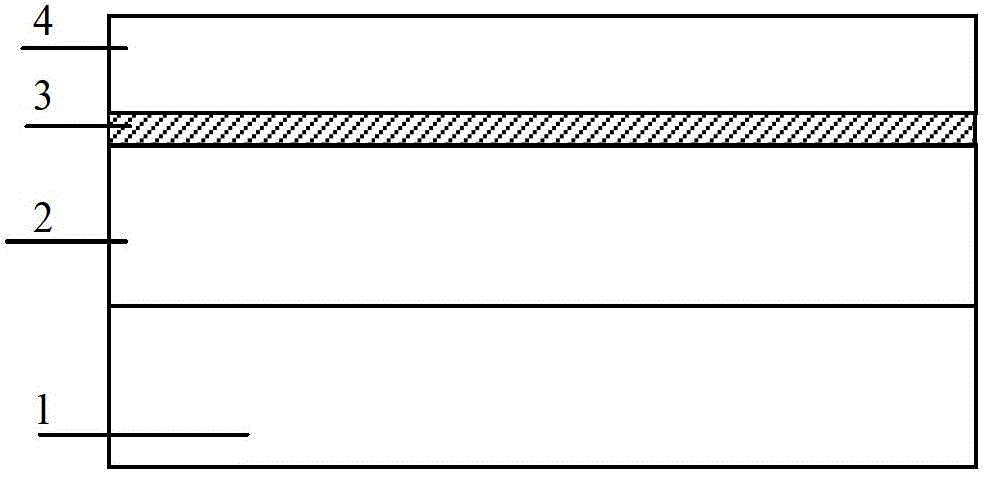
[0076] Step 1, epitaxial material preparation, as shown in Figure 2(a).

[0077] (1a) Select the doping concentration as 10 15 cm -3 Left and right P-type Si substrate sheets 1;

[0078] (1b) Using chemical vapor deposition (CVD), at 600°C, grow a layer of N-type Si epitaxial layer 2 with a thickness of 2.5 μm on the substrate as the drain region, with a doping concentration of 5×10 19 cm -3 ;

[0079] (1c) Using chemical vapor deposition (CVD), grow an N-type strained SiGe layer 3a with a thickness of 5nm on the substrate at 600°C, with a doping concentration of 5×10 17 cm -3 , the Ge composition is 10%, as the first lightly doped source and drain region (LDD) layer;

[0080] (1d) Using chemical vapor deposition (CVD), at 600°C, grow a P-type SiGe layer 3 with a thickness of 45 nm on the Si epi...

Embodiment 2

[0109] Embodiment 2: the preparation of the strained SiGe back channel NMOS integrated device and circuit with a conductive channel of 30nm, the specific steps are as follows:

[0110] Step 1, epitaxial material preparation, as shown in Figure 2(a).

[0111] (1a) Select the doping concentration to be 5×10 15 cm -3 Left and right P-type Si substrate sheets 1;

[0112] (1b) Using chemical vapor deposition (CVD), at 700°C, grow a layer of N-type Si epitaxial layer 2 with a thickness of 2.5 μm on the substrate as the drain region, with a doping concentration of 1×10 20 cm -3 ;

[0113] (1c) Using chemical vapor deposition (CVD), grow an N-type strained SiGe layer 3a with a thickness of 4nm on the substrate at 700°C, with a doping concentration of 1×10 18 cm -3 , the Ge composition is 10%, as the first lightly doped source and drain region (LDD) layer;

[0114] (1d) Using chemical vapor deposition (CVD), at 700°C, grow a P-type SiGe layer 3 with a thickness of 30 nm on the S...

Embodiment 3

[0143] Embodiment 3: the preparation of the strained SiGe back channel NMOS integrated device and circuit with a conductive channel of 22nm, the specific steps are as follows:

[0144] Step 1, epitaxial material preparation, as shown in Figure 2(a).

[0145] (1a) Select the doping concentration as 10 16 cm -3 Left and right P-type Si substrate sheets 1;

[0146] (1b) Using chemical vapor deposition (CVD), at 750°C, grow a layer of N-type Si epitaxial layer 2 with a thickness of 2 μm on the substrate as the drain region, with a doping concentration of 5×10 20 cm -3 ;

[0147] (1c) Using chemical vapor deposition (CVD), grow an N-type strained SiGe layer 3a with a thickness of 3nm on the substrate at 750°C, with a doping concentration of 5×10 18 cm -3 , the Ge composition is 10%, as the first lightly doped source and drain region (LDD) layer;

[0148] (1d) Using chemical vapor deposition (CVD), at 750°C, grow a P-type SiGe layer 3 with a thickness of 22nm on the Si epitax...


PUM

PropertyMeasurementUnit
thicknessaaaaaaaaaa
thicknessaaaaaaaaaa
thicknessaaaaaaaaaa

Abstract

The invention provides a strain SiGe square-in-square type channel NMOS (N-channel Metal Oxide Semiconductor) integrated device which is suitable for an NMOS integrated device, and a preparation method of the strain SiGe square-in-square type channel NMOS integrated device by using a micron level process. The preparation method comprises the steps of: continuously growing a Si epitaxial layer, a first strain SiGe light doping drain region (LDD) electrode layer, a strain SiGe layer, a second strain SiGe LDD region layer and an N type Si layer; forming a drain region, a source region and a drain connecting region by using technical means such as chemical vapor deposition (CVD) and dry etching and finally forming an NMOS device; and photoetching a lead to form an NMOS integrated circuit. According to the invention, under the condition of no addition of any fund and equipment input, the stain SiGe square-in-square type vertical channel NMOS integrated device which is improved in property in comparison with a body Si NMOS is manufactured at low temperature.

Description

technical field [0001] The invention belongs to the technical field of semiconductor integrated circuits, and in particular relates to a strained SiGe back-type vertical channel NMOS integrated device with a conduction channel length of 22-45 nm prepared by micron-level integrated circuit technology and a preparation method. Background technique [0002] The integrated circuit industry has a high multiplier and relevance to modern economic and social development. The development of integrated circuit technology and its industry can promote the development of consumer electronics industry, computer industry, communication industry and related industries. The development of informatization is of great significance. As the fastest-growing, most influential, and most widely used technology in human history, integrated circuits have become an important indicator of a country's scientific and technological level, comprehensive national strength, and national defense strength. Th...

Claims


Application Information

Patent Timeline
Patent Type & Authority Patents(China)
IPC IPC(8): H01L29/78H01L29/10H01L29/06H01L21/336
Inventor 胡辉勇宣荣喜张鹤鸣宋建军吕懿王海栋王斌郝跃
Owner XIDIAN UNIV
Learn More