Method for backside-contacting a silicon solar cell, and silicon solar cell with backside-contacting

A silicon solar cell and backside technology, applied in the field of solar cells, can solve the problems of surface damage of silicon chips, degradation of electrical properties of solar cells, etc., and achieve the effects of reducing the risk of chip breakage, preventing damage, and reducing manufacturing costs.

Inactive Publication Date: 2012-11-07
太阳能界先趋有限公司
View PDF4 Cites 11 Cited by
  • Summary
  • Abstract
  • Description
  • Claims
  • Application Information

AI Technical Summary

Problems solved by technology

However, ultrasonic loading and surface fusion, or thermal spraying, respectively, give high kinetic energy to the solder particles to be alloyed, which may cause damage to the silicon chip surface, thus causing degradation of the electrical properties of the solar cell

Method used


Image

  • Method for backside-contacting a silicon solar cell, and silicon solar cell with backside-contacting
  • Method for backside-contacting a silicon solar cell, and silicon solar cell with backside-contacting
  • Method for backside-contacting a silicon solar cell, and silicon solar cell with backside-contacting

Examples


Embodiment Construction

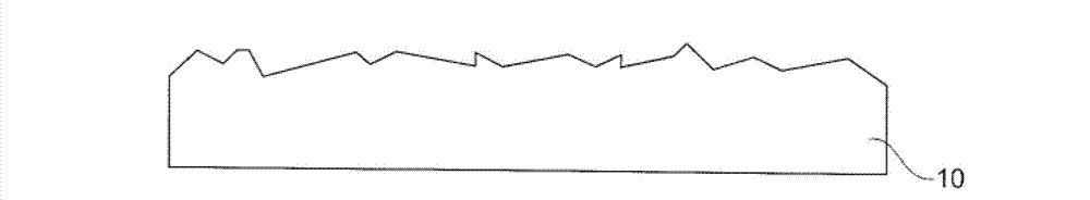
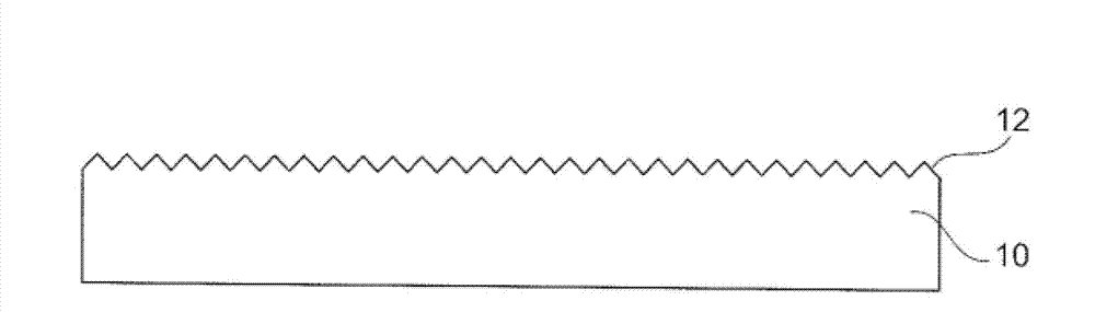
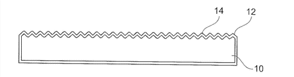
[0024] In the following, combined with Figure 1-8 To explain a possible configuration of a cheap and simple way of a method for fabricating a silicon solar cell with a back contact comprising a back surface field. Figure 9 Rear view of a silicon solar cell showing possible configurations with contact fields for back contact. Figure 10 A cutaway view showing a solar module with two solar cells connected in series. Figure 11-13 and Figure 14-17 Two further possible configurations of the method for manufacturing a silicon solar cell with an inexpensive and easily configurable back contact comprising a back surface field are respectively shown. All figures are schematic representations only and not drawn to scale.

[0025] In the method according to the invention for arranging a rear contact on a silicon solar cell, methods known from the field of semiconductors and solar technology are used. In addition, materials commonly used in the field of semiconductor and solar tech...


PUM


Abstract

The arrangement has a separation element comprising a plug fuse and a magnet, which actuates a reed relay or a reed switch. Functional coupling of signal lines of an electric energy storage is provided by a coupling element, which is galvanically separated. Power transfer lines (30) of the storage are galvanically separated by a separation unit (10) with the separation element. The coupling element is selected from a group consisting of an optocoupler, an operational amplifier with inductive or capacitive transmission, a relay and a semiconductor circuit with high-blocking transistors.

Description

technical field [0001] The invention relates to the field of solar cells, in particular to a method for back contacting a silicon solar cell and a silicon solar cell including the back contact. Background technique [0002] Typically, silicon is used as a basic material for solar cells. In the manufacture of silicon solar cells, the starting point is the crystalline silicon chip, where the p-n junction is formed using doping. To configure the p-n junction, the procedure is therefore usually to use a p-doped silicon substrate and form an n-doped emitter layer. The two ends of the p-n junction are then typically in contact via the front and back of the silicon chip. [0003] In the framework of the backside contact, so-called "back surface fields" are arranged on the backside of the silicon chip in order to prevent recombination losses. For this purpose, an aluminum layer is typically deposited on the backside of the silicon chip, covering the entire surface, and then the a...

Claims


Application Information

Patent Timeline
Patent Type & Authority Applications(China)
IPC IPC(8): H01L31/18H01L31/0224H01L31/05
CPCH01L21/283H01L31/18H01L31/0516H01L21/268H01L31/0224H01L21/24Y02E10/50H01L31/05H01L31/022441
Inventor 威蓝·碧斯哈洛·韩克利斯汀·史克雷格尔托尔斯坦·韦柏马汀·库哲
Owner 太阳能界先趋有限公司
Why Eureka
Try Eureka