Spectrum device for measuring LED (light-emitting diode) epitaxial wafer photoluminescence on line

A light-emitting diode, photoluminescence technology, applied in the direction of emission spectrum, spectrum investigation, etc., to achieve the effect of ensuring normal growth, reducing economic losses, and simple structure

Active Publication Date: 2012-11-14
南昌硅基半导体科技有限公司 +1
View PDF5 Cites 5 Cited by
  • Summary
  • Abstract
  • Description
  • Claims
  • Application Information

AI Technical Summary

Problems solved by technology

[0003]However, there are some technical difficulties to be overcome in order to realize online photoluminescence spectrum measurement
The first reason is that the PL at high temperature is relatively weak and difficult to measure; the second reason is that there is no suitable laser for excitation before; the third reason is that the photoluminescence signal of the epitaxial wafer is in the reaction chamber, and the excitation of the luminescence spectrum is consistent with It's hard to collect
For these reasons, there are no scientific research reports in this area, let alone instruments and equipment in this area.

Method used


Image

  • Spectrum device for measuring LED (light-emitting diode) epitaxial wafer photoluminescence on line
  • Spectrum device for measuring LED (light-emitting diode) epitaxial wafer photoluminescence on line
  • Spectrum device for measuring LED (light-emitting diode) epitaxial wafer photoluminescence on line

Examples


Embodiment 1

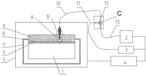
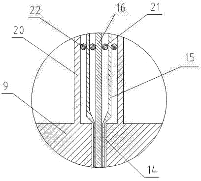
[0020] An on-line device for measuring the photoluminescence spectrum of a light-emitting diode epitaxial wafer includes a reaction chamber 7 and a control system 4 , and an MOCVD heater 1 is installed in the reaction chamber 7 placed in a glove box 5 . A graphite base 6 and an epitaxial wafer 8 are installed sequentially from bottom to top on the MOCVD heater 1 , the MOCVD heater 1 heats and controls the temperature of the graphite base 6 , and the graphite base 6 heats the epitaxial wafer 8 . On the top of the reaction chamber 7, an MOCVD shower head 9 facing the epitaxial wafer 8 and spaced from the epitaxial wafer 8 is installed. A quartz rod assembly hole 14 perpendicular to the epitaxial wafer 8 and penetrating is processed on the MOCVD shower head 9. The quartz rod assembly It consists of a quartz rod 16 and a quartz rod jacket 15 that is covered on the outer wall of the quartz rod 16. An outer sealing metal tube 20 is provided on the top of the outer wall of the MOCVD n...

Embodiment 2

[0029] The structure of embodiment 2 is basically the same as embodiment 1, the difference is:

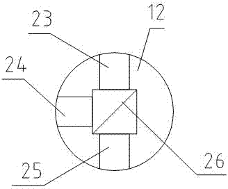
[0030] exist Figure 5 In, use Y-shaped fiber block 28 to replace the whole Figure 4 The fiber branch block 12 in the part, the Y-shaped fiber block 28 is made up of dry fiber 27, spectrum fiber 11 and laser fiber 13, and dry fiber 27 is exactly to form by combining spectrum fiber 11, laser fiber 13 in fact, and then jointly with quartz rod The end face of 16 realizes the coupling, and even cancels the quartz rod 16, and directly extends the two optical fibers into the reaction chamber 7, and at this time, vacuum seals between the optical fibers and the reaction chamber. The coupling efficiency of using the Y-shaped fiber block 28 will be reduced by at least a factor of 1, although it is convenient.

[0031]In order to prevent the laser light reflected by the epitaxial wafer 8 (containing the film thickness information of the epitaxial wafer) from entering the fiber optic spectr...


PUM


Abstract

The invention discloses a spectrum device for measuring LED (light-emitting diode) epitaxial wafer photoluminescence on line. The spectrum device for measuring LED epitaxial wafer photoluminescence on line comprises a reaction chamber and a control system, an MOCVD (metal organic chemical vapor deposition) heater, a graphite substrate base, an epitaxial wafer and an MOCVD spray nozzle are installed in the reaction chamber. The device for measuring LED epitaxial wafer photoluminescence spectra on line is characterized in that a quartz rod and a quartz outer sleeve are installed in a quartz rod hole of the MOCVD spray nozzle; a laser optical fiber is connected between a laser device and a laser emission collimation head; a multiplex optical fiber is connected between an excitation receiving collimation head and the quartz rod; a spectrum optical fiber is connected between a spectrum collimation head and an optical fiber spectrometer; and the control system controls the reaction chamber, the laser device and the optical fiber spectrometer. According to the invention, the signal intensity of photoluminescence is improved through reducing the temperature of the epitaxial wafer artificially, and then the photoluminescence spectra are excited and collected through the quartz rod, and are displayed on the optical fiber spectrometer; and the spectrum device for measuring LED epitaxial wafer photoluminescence on line has the advantages the growth situation of the epitaxial wafer in the reaction chamber can be monitored in real time, the normal growth of the epitaxial wafer can be guaranteed, economic loss can be reduced and the like.

Description

technical field [0001] The invention relates to semiconductor material manufacturing equipment, in particular to a device capable of on-line measuring the photoluminescent spectrum of a light-emitting diode epitaxial wafer. Background technique: [0002] At present, a large-scale energy-saving and emission-reduction movement is emerging all over the world. Semiconductor lighting (that is, using light-emitting diodes (LED) lighting) is one of the effective measures. However, if it is to enter thousands of households in China, the cost must be greatly reduced. . An effective measure to reduce costs is to improve the controllability of epitaxial production. For this reason, it is very important to monitor various parameters of epitaxial production on-line. Metal organic chemical vapor deposition equipment (MOCVD) is an important equipment for preparing semiconductor materials. At present, the temperature of the epitaxy, the thickness of the epitaxial layer, and the stress s...

Claims


Application Information

Patent Timeline
Patent Type & Authority Applications(China)
IPC IPC(8): G01J3/443
Inventor 方文卿刘苾雨江风益
Owner 南昌硅基半导体科技有限公司
Why Eureka
Try Eureka