Production method of gallium nitride (GaN)-based light emitting diode (LED) chip with indium tin oxide (ITO) surface roughness

A technology of LED chip and surface roughening, which is used in electrical components, circuits, semiconductor devices, etc.

Active Publication Date: 2012-11-21
YANGZHOU ZHONGKE SEMICON LIGHTING
View PDF5 Cites 12 Cited by
  • Summary
  • Abstract
  • Description
  • Claims
  • Application Information

AI Technical Summary

Problems solved by technology

[0003] Aiming at the difficulties and problems existing in the existing roughened ITO, the purpose of th

Method used


Image

  • Production method of gallium nitride (GaN)-based light emitting diode (LED) chip with indium tin oxide (ITO) surface roughness
  • Production method of gallium nitride (GaN)-based light emitting diode (LED) chip with indium tin oxide (ITO) surface roughness
  • Production method of gallium nitride (GaN)-based light emitting diode (LED) chip with indium tin oxide (ITO) surface roughness

Examples


Embodiment Construction

[0034] 1. Making LED chips:

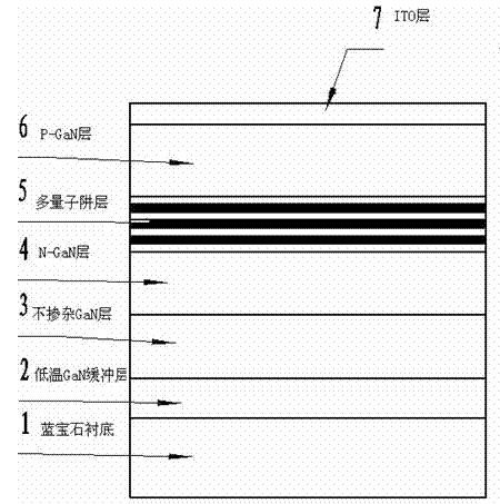
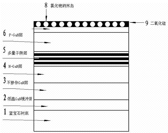
[0035] Step 1: Using metal-organic chemical vapor deposition (MOCVD), sequentially grow 1 μm low-temperature GaN buffer layer 2, 2 μm undoped GaN layer 3, 2 μm N-GaN layer 4, and 250 nm multi-quantum well light emission on the semiconductor substrate 1 Layer 5 and 300nm P-GaN layer 6 to form a GaN epitaxial wafer.

[0036] The aforementioned semiconductor substrate 1 can be any one of sapphire, silicon, silicon carbide or metal.

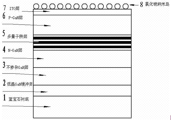
[0037] Step 2: Prepare an ITO thin film layer on the upper surface of the P-GaN layer 6 of the GaN epitaxial wafer, with a thickness of 500-9000 Å, such as figure 1 shown.

[0038] Step 3: Process the surface of the ITO thin film layer 7 to make a nano-bowl-shaped roughened surface, the following steps:

[0039] (1) Put the GaN epitaxial wafer covered with the ITO thin film layer 7 into the evaporation table, and evaporate a cesium chloride thin film on the surface of the ITO thin film layer 7 for 5 to 40 minutes. The...


PUM

PropertyMeasurementUnit
Thicknessaaaaaaaaaa
Diameteraaaaaaaaaa
Etching poweraaaaaaaaaa

Abstract

The invention relates to a production method of a gallium nitride (GaN)-based light emitting diode (LED) chip with indium tin oxide (ITO) surface roughness, which relates to the technical field of the production of a semiconductor. The production method comprises following steps of firstly forming a GaN epitaxial wafer; preparing an ITO film layer on the surface of a phosphorus gallium nitride (P-GaN) layer of the epitaxial wafer; roughening the surface of the film layer; performing inductively coupled plasma (ICP) etching on one side of the GaN epitaxial wafer, and forming an ITO transparent electrode on a P-type table-board; forming a positive (P) electrode and a negative (N) electrode; and thinning a semiconductor substrate, and then slicing the semiconductor substrate into independent chips. The production method is characterized in that when the surface roughening is performed on the surface of the ITO film layer, a nano bowl-shaped roughened surface layer is produced, and the nano bowl-shaped roughened surface layer is formed by joining a plurality of back surfaces respectively to bowl-shaped grooves on the P-GaN layer, wherein the back surfaces are connected with each other. The size and the depth of each bowl-shaped groove in the nano bowl-shaped roughened surface layer are controllable, and the bowl-shaped structure is more favorable for the light extraction.

Description

technical field [0001] The invention relates to the technical field of semiconductor production. Background technique [0002] In the GaN-based front-mount LED structure, indium tin oxide (ITO) transparent conductive film is usually used as the current spreading layer of the P mesa. The refractive index of ITO is about 2, and the critical angle of total reflection between the ITO interface and air is 30°. Only a small amount of the light generated in the region escapes out of the ITO. This requires designing the chip structure to reduce total reflection and increase the critical angle of the escape light cone. Now the industry usually adopts ITO surface roughening technology to reduce the total reflection of outgoing light, so as to improve the light extraction efficiency. However, it is more difficult to roughen the ITO, and the preparation and removal of the roughening mask are more difficult. Contents of the invention [0003] In view of the difficulties and problems...

Claims


Application Information

Patent Timeline
IPC IPC(8): H01L33/22H01L33/00
Inventor 李璟王国宏詹腾
Owner YANGZHOU ZHONGKE SEMICON LIGHTING
Why Eureka
Try Eureka