Rear-contact heterojunction photovoltaic cell

A photovoltaic cell and back surface technology, applied in photovoltaic power generation, circuits, electrical components, etc., to achieve the effects of simplified manufacturing process, good passivation, and small ohmic loss

Inactive Publication Date: 2012-11-21
TOTAL MARKETING SERVICES SA +1
View PDF12 Cites 3 Cited by
  • Summary
  • Abstract
  • Description
  • Claims
  • Application Information

AI Technical Summary

Problems solved by technology

[0011] A disadvantage of all these devices is that their fabrication requires two separate steps of depositing the amorphous silicon, for example using a mask in each step, or first depositing one amorphous silicon and then etching the already deposited amorphous silicon before depositing the other. deposited amorphous silicon

Method used


Image

  • Rear-contact heterojunction photovoltaic cell
  • Rear-contact heterojunction photovoltaic cell
  • Rear-contact heterojunction photovoltaic cell

Examples


Embodiment Construction

[0061] In the following description, the invention will be described in more detail without limitation with reference to photovoltaic applications of the invention.

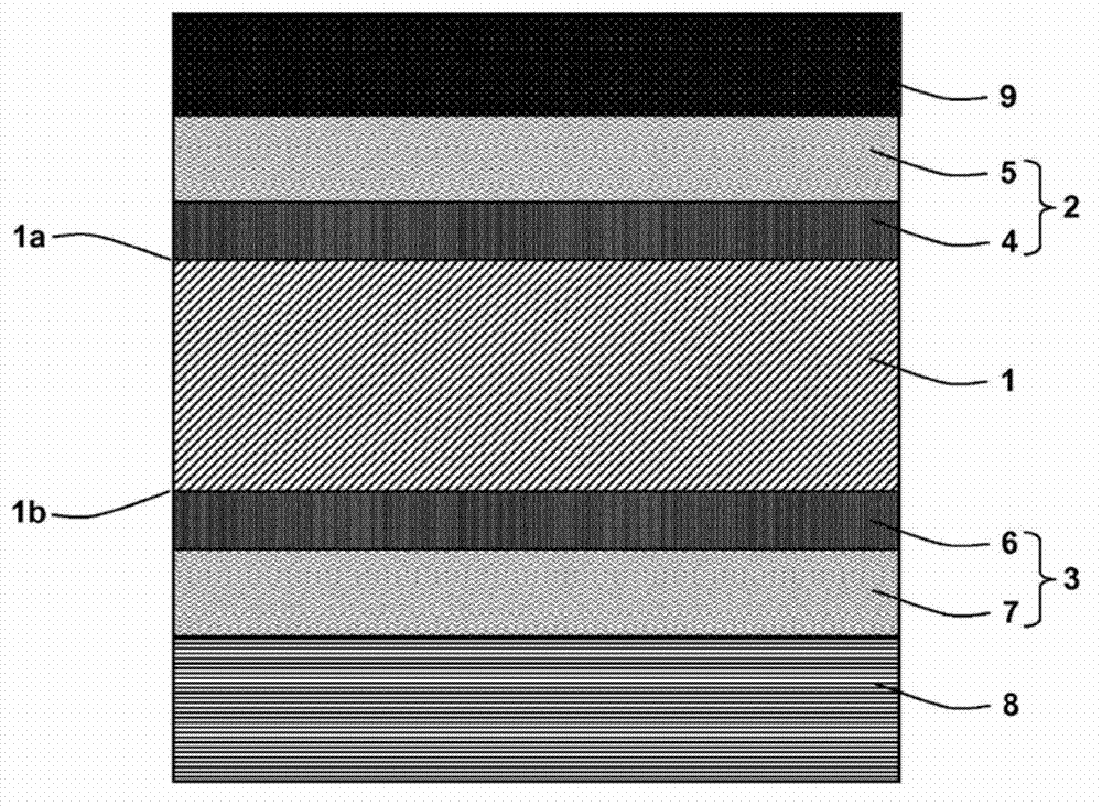
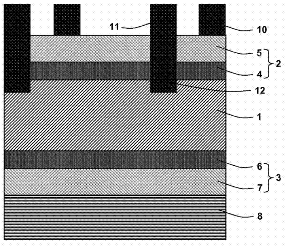
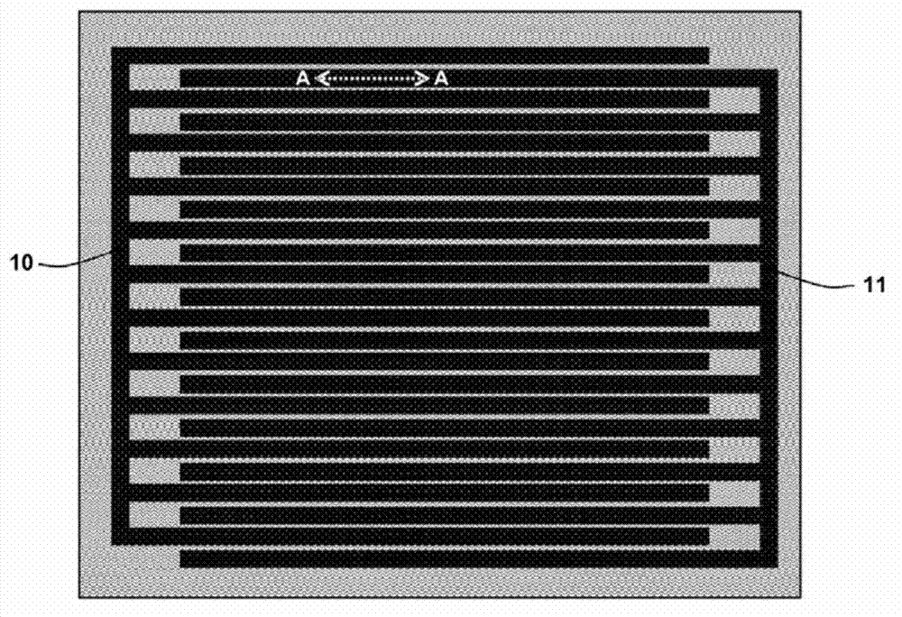
[0062] see figure 1 , the semiconductor device according to the present invention can be fabricated as follows.

[0063] First, a crystalline semiconductor substrate 1 having a front surface 1a and a back surface 1b is provided. Preferably, the crystalline semiconductor substrate 1 is a crystal, especially a monocrystalline or polycrystalline (preferably monocrystalline) silicon substrate (or wafer) in the form of a wafer.

[0064] The substrate can be doped n-type or p-type. The use of n-type doped substrates is particularly advantageous due to their longer lifetime. In the following, an n-type doped substrate is taken as an example. Advantageously, the substrate 1 does not have any oxide material.

[0065] Preferably, the substrate 1 has sufficient doping to have a resistivity between about 0.1 and 1 Ω·cm....


PUM


Abstract

The invention relates to a semiconductor device comprising: a crystalline semiconductor substrate (1) having a front face (1a) and a rear face (1b); a front passivation layer (3) placed on the front face (1a) of the substrate (1); a rear passivation layer (2) placed on the rear face (1b) of the substrate (1); a first metallization zone (10) placed on the rear passivation layer (2) and designed for collecting electrons; a second metallization zone designed for collecting holes, comprising: a surface portion (11) placed on the rear passivation layer (2); and an internal portion (12) passing through the rear passivation layer (2) and forming, in the substrate (1), a region in which the concentration of electron acceptors is greater than the rest of the substrate (1). The invention also relates to a module of photovoltaic cells using this device and to a process for manufacturing this device.

Description

technical field [0001] The present invention relates to a back contact heterojunction photovoltaic cell, and also relates to a manufacturing process of the back contact heterojunction photovoltaic cell. Background technique [0002] As currently known, a photovoltaic module comprises a plurality of photovoltaic cells (or solar cells) connected in series and / or in parallel. Photovoltaic cells are semiconductor diodes designed to absorb light energy and convert it into electricity. The semiconductor diode comprises a p-n junction between two layers, p-type doped silicon and n-type doped silicon, respectively. During the formation of this junction, a potential difference (and thus a local electric field) arises due to the excess of free electrons in the n-layer and due to the scarcity of free electrons in the p-layer. [0003] When photons are absorbed by the semiconductor, they release their energy to generate free electrons and holes. Considering the potential difference p...

Claims


Application Information

Patent Timeline
Patent Type & Authority Applications(China)
IPC IPC(8): H01L31/0224H01L31/0352
CPCH01L31/072Y02E10/52H01L31/02167H01L31/022441Y02E10/50H01L31/02168H01L31/0368H01L31/0376H01L31/0504H01L31/1864H01L31/1868
Inventor P.罗卡伊卡巴洛卡斯M.拉布龙
Owner TOTAL MARKETING SERVICES SA
Why Eureka
Try Eureka