Method for preparing photoresist template and patterned ZnO nanorod array

A nanorod array and photoresist technology, which is applied in the photoengraving process of the pattern surface, optomechanical equipment, originals for optomechanical processing, etc. Asymmetric structure and other problems, to achieve the effect of simple structure, fast processing speed, and small damage to the template

Active Publication Date: 2013-11-20
UNIV OF SCI & TECH BEIJING
View PDF8 Cites 3 Cited by
  • Summary
  • Abstract
  • Description
  • Claims
  • Application Information

AI Technical Summary

Problems solved by technology

[0008] However, a single exposure with two-beam laser interference can only produce a linear template. To generate a hole template, multiple rotational exposures are required, twice for a square arrangement, and three times for a hexagonal arrangement.
This method of multiple exposures has the following disadvantages: 1. Time-consuming and laborious, and prolonging the action time of the external environment, it is easy to reduce the quality of the hole template; The structure will appear asymmetrical; 3. When preparing the hexagonal hole template with three exposures, Moiré fringes are prone to appear, resulting in a large number of holes being closed
Adjusting the position and direction of M1, M2 and M3 can realize the above two kinds of three-beam interference lithography, but this method has problems such as complicated equipment and small processing area.

Method used


Image

  • Method for preparing photoresist template and patterned ZnO nanorod array
  • Method for preparing photoresist template and patterned ZnO nanorod array
  • Method for preparing photoresist template and patterned ZnO nanorod array

Examples


Embodiment 1

[0038] The preparation of the photoresist template comprises the following preparation steps:

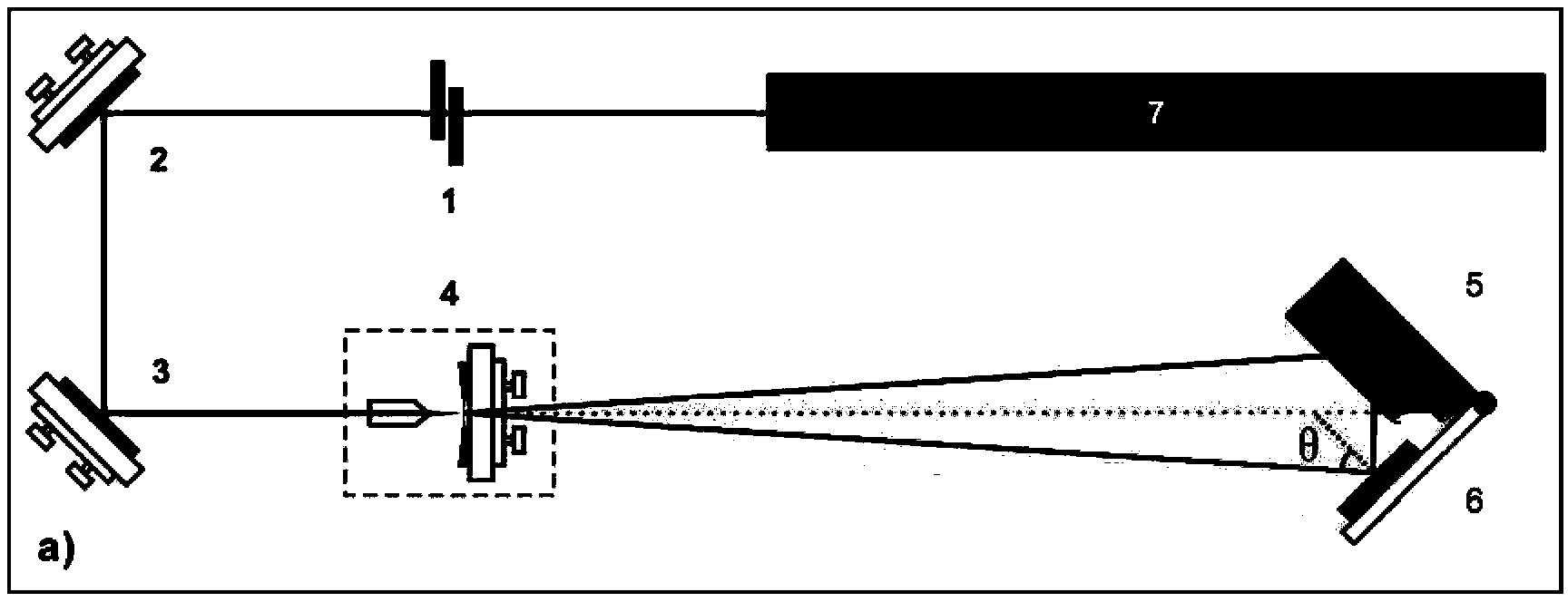
[0039] (1) Three-beam laser interference system construction: such as figure 1 As shown, a beam of 325nm laser is emitted from the He-Cd laser (7), reflected by two dielectric total reflection mirrors (2, 3), and enters the spatial filter (4) for filtering processing. The objective lens with a focal length of 2 cm and a diameter It consists of a pinhole of 5 μm, and then expands the beam by 100 cm to form a large spot with a diameter of 12 cm; the sample stage (6) is placed at an incident angle of 18.5 degrees, and the two 5×10 cm square UV-enhanced aluminum mirrors (5) have a mutual angle of 120 degrees and are perpendicular to the sample stage, the intersection of the sample stage (6) and the two mirrors is aligned with the center of the large spot; an electronic shutter (1) is placed to precisely control the exposure time.

[0040] (2) Substrate cleaning and photoresist spin coa...

Embodiment 2

[0043] The preparation method of p-GaN substrate patterned ZnO nanorod array, comprises the following steps:

[0044] (1) Three-beam laser interference system construction: such as figure 1 As shown, a beam of 325nm laser is emitted from the He-Cd laser (7), reflected by two dielectric total reflection mirrors (2, 3), and enters the spatial filter (4) for filtering processing. The objective lens with a focal length of 2 cm and a diameter It consists of a pinhole of 5 μm, and then expands the beam by 100 cm to form a large spot with a diameter of 12 cm; the sample stage (6) is placed at an incident angle of 5 degrees, and the two 5×10 cm square UV-enhanced aluminum reflectors (5) have a mutual angle of 120 degrees and are perpendicular to the sample stage, the intersection of the sample stage (6) and the two mirrors is aligned with the center of the large spot; an electronic shutter (1) is placed to precisely control the exposure time.

[0045] (2) Substrate cleaning and photo...

Embodiment 3

[0050] Si substrate patterned ZnO nanorod arrays

[0051] (1) Three-beam laser interference system construction: such as figure 1 As shown, a beam of 325nm laser is emitted from the He-Cd laser (7), reflected by two dielectric total reflection mirrors (2, 3), and enters the spatial filter (4) for filtering processing. The objective lens with a focal length of 2 cm and a diameter It consists of a pinhole of 5 μm, and then expands the beam by 100 cm to form a large spot with a diameter of 12 cm; the sample stage (6) is placed at an incident angle of 60 degrees, and the two 5×10 cm square UV-enhanced aluminum reflectors (5) have a mutual angle of 120 degrees and are perpendicular to the sample stage, the intersection of the sample stage (6) and the two mirrors is aligned with the center of the large spot; an electronic shutter (1) is placed to precisely control the exposure time.

[0052] (2) Substrate cleaning, seed layer sputtering and photoresist spin coating: 1×1cm Si substr...


PUM

PropertyMeasurementUnit
diameteraaaaaaaaaa

Abstract

The invention discloses a method for preparing a photoresist template by using three-beam laser interference and application of a patterned ZnO nanorod array prepared by using the method. According to the method, a large-area hexagonal-arranged circular-hole template is quickly formed through single-time exposure by virtue of a three-beam laser interference patterning technology, and the accurate regulation and control on the position, thickness, length and density of ZnO nanorods are realized through carrying out confinement hydrothermal growth on a ZnO nanorod array by using the template, so that the method has the advantages of simple system and structure, low cost, no need of a mask and a turntable, high processing speed, strong ability of regulation and control, and the like. The obtained large-area height-orderly-arranged ZnO nanorod array can be applied to multiple related fields, including light emitting diodes, ultraviolet detectors, dye-sensitized solar cells, field emission cold cathodes, stress sensors, biosensors and the like, and finally, the performance of nano-functional devices is improved, so that the ZnO nanorod array has great practical significance.

Description

technical field [0001] The invention belongs to the field of patterned growth of nanometer materials, and in particular relates to a method for preparing a photoresist template by three-beam laser interference and an application of the method for preparing a patterned ZnO nanorod array. Background technique [0002] ZnO nanorod array is one of the most widely and deeply researched materials in the ZnO nanomaterial system. It not only has the electro-optical characteristics of ZnO nanomaterials, but also has the advantages of high specific surface area and easy low-cost large-area production. and Zhong Lin Wang, Nature Nanotechnology, vol5, May 2010), electrodynamic sensors ([2] Min‐Yeol Choi, Dukhyun Choi, Mi‐Jin Jin, Insoo Kim, Sang‐Hyeob Kim, Jae‐Young Choi, Sang Yoon Lee, Jong Min Kim, and Sang‐Woo Kim, Adv. Mater. 2009, 21, 2185‐2189), Light Emitting Diodes ([3] Xiao‐Mei Zhang, Ming‐Yen Lu, Yue Zhang, Lih‐J. Chen, and Zhong Lin Wang, Adv. Mater.2009, 21, 2767‐2770), fi...

Claims


Application Information

Patent Timeline
Patent Type & Authority Patents(China)
IPC IPC(8): G03F7/00G03F1/76B81C1/00
Inventor 张跃陈翔闫小琴李欣冯亚瀛郑鑫申衍伟
Owner UNIV OF SCI & TECH BEIJING
Why Eureka
Try Eureka