Dual-strain bipolar complementary metal-oxide semiconductor (BiCMOS) integration device based on silicon on insulator (SOI) substrate and preparation method thereof

An integrated device and dual-strain technology, applied in semiconductor/solid-state device manufacturing, electric solid-state devices, semiconductor devices, etc., can solve problems that affect device performance, reduce lithography precision, and lithography technology cannot meet

Inactive Publication Date: 2012-12-05
XIDIAN UNIV
View PDF3 Cites 0 Cited by
  • Summary
  • Abstract
  • Description
  • Claims
  • Application Information

AI Technical Summary

Problems solved by technology

For example, when the feature size is less than 100nm, due to problems such as tunneling leakage current and reliability, the traditional gate dielectric material SiO 2 Unable to meet the requirements of low power consumption; the short channel effect and narrow channel effect of na

Method used


Image

  • Dual-strain bipolar complementary metal-oxide semiconductor (BiCMOS) integration device based on silicon on insulator (SOI) substrate and preparation method thereof

Examples


Embodiment 1

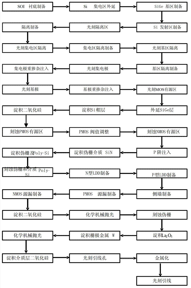
[0112] Embodiment 1: The channel length is prepared as the double-strained plane BiCMOS integrated device and circuit based on SOI substrate with a channel length of 22nm. The specific steps are as follows:

[0113] Step 1, preparation for epitaxial growth.

[0114] (1a) Select the SOI substrate, the support material of the lower layer of the substrate is Si, and the middle layer is SiO 2 , with a thickness of 150nm, and the upper material is doped with a concentration of 1×10 16 cm -3 N-type Si with a thickness of 100nm;

[0115] (1b) Using the chemical vapor deposition (CVD) method, at 600 ° C, grow a layer of N-type epitaxial Si layer with a thickness of 50 nm on the upper Si material, as the collector region, and the doping concentration of this layer is 1× 10 16 cm -3 ;

[0116] (1c) Using chemical vapor deposition (CVD), grow a SiGe layer with a thickness of 20nm on the substrate at 600°C. As the base region, the Ge composition of this layer is 15%, and the doping ...

Embodiment 2

[0172] Embodiment 2: preparation of dual-strained plane BiCMOS integrated device and circuit based on SOI substrate with a channel length of 130nm, the specific steps are as follows:

[0173] Step 1, preparation for epitaxial growth.

[0174] (1a) Select the SOI substrate, the support material of the lower layer of the substrate is Si, and the middle layer is SiO 2 , with a thickness of 300nm, and the upper material is doped with a concentration of 5×10 16 cm -3 N-type Si with a thickness of 120nm;

[0175] (1b) Using chemical vapor deposition (CVD), grow an N-type epitaxial Si layer with a thickness of 80nm on the upper Si material at 700°C as the collector region, and the doping concentration of this layer is 5× 10 16 cm -3 ;

[0176] (1c) Using chemical vapor deposition (CVD), grow a layer of SiGe layer with a thickness of 40nm on the substrate at 700°C. As the base region, the Ge composition of this layer is 20%, and the doping concentration is 1×10 19 cm -3 ;

...

Embodiment 3

[0232] Embodiment 3: preparation channel length is 350nm based on double strain plane BiCMOS integrated device and circuit of SOI substrate, concrete steps are as follows:

[0233] Step 1, preparation for epitaxial growth.

[0234] (1a) Select the SOI substrate, the support material of the lower layer of the substrate is Si, and the middle layer is SiO 2 , with a thickness of 400nm, and the upper material is doped with a concentration of 1×10 17 cm -3 N-type Si with a thickness of 150nm;

[0235] (1b) Using the method of chemical vapor deposition (CVD), grow a layer of N-type epitaxial Si layer with a thickness of 100nm on the upper layer of Si material at 750°C, as the collector region, and the doping concentration of this layer is 1× 10 17 cm -3 ;

[0236] (1c) Using chemical vapor deposition (CVD), grow a layer of SiGe layer with a thickness of 60nm on the substrate at 750°C. As the base region, the Ge composition of this layer is 25%, and the doping concentration is ...


PUM

PropertyMeasurementUnit
Thicknessaaaaaaaaaa
Thicknessaaaaaaaaaa
Thicknessaaaaaaaaaa

Abstract

The invention discloses a dual-strain bipolar complementary metal-oxide semiconductor (BiCMOS) integration device based on a silicon on insulator (SOI) substrate and a preparation method thereof. The preparation method comprises following steps that a negative-silicon (N-Si) layer, a positive-silicon germanium (P-SiGe) layer and an N-Si layer continuously grow on the SOI substrate, a deep groove isolator is prepared, a collector zone shallow groove isolator and a base zone shallow groove isolator are prepared, a collector zone is photo-etched, phosphonium ions are injected to form a collector electrode, a base electrode and a transmitter electrode, and a SiGe heterojunction bipolar transistor (HBT) device is formed; a strain SiGe material grow on the substrate, an N-channel MOS (NMOS) device active region and a P-channel MOS (PMOS) device active region are formed, a pseudo grid is prepared, a source drain region of the NMOS and the PMOS devices is respectively generated in a self-aligning way, the pseudo grid is eliminated, a lanthanum oxide (La2O3) material is prepared in a pressing groove at the pseudo grid to form a grid medium and metal tungsten (W) to form a grid electrode, a lead is photo-etched, and a dual-strain plane BiCMOS integration device and a circuit based on the SOI substrate are formed. According to the method, the characteristic that a hole mobility of the strain SiGe material is higher than that of the bulk-Si material is adequately utilized to prepare the dual-strain plane BiCMOS integration circuit based on the SOI substrate, so that the performance of the existing analog and digital-analog mixed integrated circuit is greatly improved.

Description

technical field [0001] The invention belongs to the technical field of semiconductor integrated circuits, and in particular relates to an SOI substrate-based dual-strain plane BiCMOS integrated device and a preparation method. Background technique [0002] Semiconductor integrated circuit technology is the core technology of high-tech and information industries, and has become an important symbol to measure a country's scientific and technological level, comprehensive national strength and national defense strength, while microelectronic technology represented by integrated circuits is the key to semiconductor technology. The semiconductor industry is the basic industry of the country. The reason why it develops so fast is not only the huge contribution of technology itself to economic development, but also its wide applicability. [0003] Gordon Moore, one of the founders of Intel, proposed "Moore's Law" in 1965, which states that the number of transistors on an integrated ...

Claims


Application Information

Patent Timeline
IPC IPC(8): H01L27/12H01L21/84
Inventor 张鹤鸣周春宇宋建军舒斌胡辉勇宣荣喜戴显英郝跃
Owner XIDIAN UNIV
Why Eureka
Try Eureka