Preparation method of one-dimensional silicon nanowires with different linear densities

A technology of silicon nanowires and silicon nanowire arrays, which is applied in the field of photocatalytic materials, can solve the problems of reduced photoelectric conversion efficiency, poor photoelectric performance of photocurrent characteristics, and easy contamination of the surface, and achieves low cost, simple and convenient preparation process, The effect of simple materials

Inactive Publication Date: 2012-12-12
NANJING UNIV OF AERONAUTICS & ASTRONAUTICS
View PDF2 Cites 11 Cited by
  • Summary
  • Abstract
  • Description
  • Claims
  • Application Information

AI Technical Summary

Problems solved by technology

Studies have shown that the narrow bandgap of silicon leads to the recombination of photogenerated electrons and holes, which reduces the photoelectric conversion efficiency. Nanotechnology is an effective way to solve this problem.
However, although silicon nanomaterials have a large specific surface area, their surface is easily polluted, and when immersed in an aqueous solution, it is easy to ad

Method used


Image

  • Preparation method of one-dimensional silicon nanowires with different linear densities
  • Preparation method of one-dimensional silicon nanowires with different linear densities
  • Preparation method of one-dimensional silicon nanowires with different linear densities

Examples


Example Embodiment

[0021] Example 1:

[0022] 1) Pretreatment of silicon wafers: After cutting the silicon wafers, first place them in acetone solution to clean the ultrasonic wave, clean them with deionized water, and then immerse them in HF / H with a volume ratio of 1:10. 2 After removing the thin oxide layer in a solution of O for 15 min, blow it dry with hydrogen;

[0023] 2) One-dimensional SiNWs arrays were prepared by metal-catalyzed corrosion method, which was divided into the following two steps:

[0024] The first step is to deposit silver nanoparticles: the pretreated silicon wafer is mixed with 0.14 mol / L HF and 0.01 mol / L AgNO 3 Immerse in the mixed solution for 30s;

[0025] The second step, metal-assisted etching: the silicon substrate deposited with silver nanoparticles was immersed in HF-H 2 o 2 -H 2 In the mixed etching solution with O volume ratio of 20:10:70, etch at room temperature for 30 min, 10% SiNWs were obtained;

[0026] 3) Post-processing of one-dimensional SiNW...

Example Embodiment

[0028] Example 2:

[0029] 1), the pretreatment of silicon wafer (same as embodiment 1);

[0030] 2) One-dimensional SiNWs arrays were prepared by metal-catalyzed corrosion method, which was divided into the following two steps:

[0031] The first step is to deposit silver nanoparticles: the pretreated silicon wafer is mixed with 0.14 mol / L HF and 0.01 mol / L AgNO 3 Immerse in the mixed solution for 30s;

[0032] The second step, metal-assisted etching: the silicon substrate deposited with silver nanoparticles was immersed in HF-H 2 o 2 -H 2 In the mixed etching solution with O volume ratio of 20:20:60, etch at room temperature for 30 min, 20% SiNWs were obtained;

[0033] 3), one-dimensional SiNWs array post-processing (same as Example 1);

[0034] 4), sample characterization and photoelectric performance test (same as Example 1).

Example Embodiment

[0035] Example 3:

[0036] 1), the pretreatment of silicon wafer (same as embodiment 1);

[0037] 2) One-dimensional SiNWs arrays were prepared by metal-catalyzed corrosion method, which was divided into the following two steps:

[0038]The first step is to deposit silver nanoparticles: the pretreated silicon wafer is mixed with 0.14 mol / L HF and 0.01 mol / L AgNO 3 Immerse in the mixed solution for 30s;

[0039] The second step, metal-assisted etching: the silicon substrate deposited with silver nanoparticles was immersed in HF-H 2 o 2 -H 2 In the mixed etching solution with O volume ratio of 20:30:50, etch at room temperature for 30 min, 30% SiNWs were obtained;

[0040] 3), one-dimensional SiNWs array post-processing (same as Example 1);

[0041] 4), sample characterization and photoelectric performance test (same as Example 1).

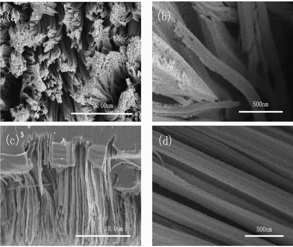
[0042] It can be seen from the SEM image that 10% H 2 o 2 The length of one-dimensional SiNWs prepared by etching is about 16 μm, and the ...


PUM

PropertyMeasurementUnit
Lengthaaaaaaaaaa
Diameteraaaaaaaaaa

Abstract

The invention discloses a preparation method of one-dimensional silicon nanowires with different linear densities. The method includes following steps of, a, preprocessing a silicon chip; b, preparing a one-dimensional silicon nanowire array by means of a metal catalysis etching method; and c, performing postprocessing, wherein the metal catalysis etching method includes two steps of, step one, depositing silver nanoparticles: impregnating the preprocessed silicon chip in an HF-AgNO3 mixed aqueous solution for 20-40 seconds, the concentration of HF is 0.1-0.2 mol/L, and the concentration of AgNO3 is 0.008-0.012 mol/L; and step two, performing metal assisted etching: immersing the silicon chip obtained from the step one into an HF-H2O2 mixed etching solution, and performing etching for 20-40 minutes under a room temperature. According to the preparation method of the one-dimensional silicon nanowires with the different linear densities, the photoelectric properties of the prepared one-dimensional silicon nanowire array are obviously improved in ultraviolet diffuse reflection, photocurrent characteristics and photocatalysis reaction, technological parameters can be adjusted to control shapes and densities of the silicon nanowires, and the preparation method is simple, low in cost and pollution-free.

Description

technical field [0001] The invention belongs to the field of photocatalytic materials, in particular to a preparation method of one-dimensional silicon nanowire (SiNWs) arrays with different line densities. Background technique [0002] Environmental pollution and energy shortage are major challenges facing mankind. The photocatalytic process can convert the inexhaustible low-density sunlight energy into high-density chemical energy and electrical energy, and can also directly use the physical and chemical changes that occur when sunlight interacts with photocatalytic materials to degrade mineralized water and air. Therefore, photocatalysis shows great potential in environmental purification and new energy development. Photocatalytic materials have high catalytic activity and stability, low price, and environmental friendliness, and have great potential in the field of environmental pollution control. In recent years, on the semiconductor TiO 2 Studies have shown that it ...

Claims


Application Information

Patent Timeline
IPC IPC(8): C01B33/021B82Y30/00
Inventor 姬广斌刘有松汪俊逸梁渲祺张兴淼
Owner NANJING UNIV OF AERONAUTICS & ASTRONAUTICS
Why Eureka
Try Eureka