Method for preparing nanometer silicon film through intermediate-frequency magnetron sputtering process, and its special device

A technology of nano-silicon film and magnetron sputtering, which is applied in nanotechnology, nanotechnology, nanotechnology for materials and surface science, etc., can solve the problem of difficult to obtain nano-silicon film, unfavorable disordered silicon network relaxation, silicon Problems such as grain nucleation and growth difficulties, to achieve good thermal stability, wide-range controllable thin film crystal structure, and improve the effect of uneven heating

Inactive Publication Date: 2014-02-05
INST OF METAL RESEARCH - CHINESE ACAD OF SCI
View PDF2 Cites 0 Cited by
  • Summary
  • Abstract
  • Description
  • Claims
  • Application Information

AI Technical Summary

Problems solved by technology

Magnetron sputtering deposition is mainly atomic deposition, and the energy of particles deposited on the substrate is relatively small. However, when depositing silicon thin films by intermediate frequency magnetron sputtering, the mobility of adsorbed silicon atoms on the substrate surface will be further affected due to the fast deposition rate. Then it reaches the limit of the silicon particles on the substrate, which is not conducive to the relaxation of the disordered silicon network, and the nucleation and growth of silicon grains are difficult, so it is difficult to obtain an ideal nano-silicon film

Method used


Image

  • Method for preparing nanometer silicon film through intermediate-frequency magnetron sputtering process, and its special device
  • Method for preparing nanometer silicon film through intermediate-frequency magnetron sputtering process, and its special device
  • Method for preparing nanometer silicon film through intermediate-frequency magnetron sputtering process, and its special device

Examples


Embodiment 1

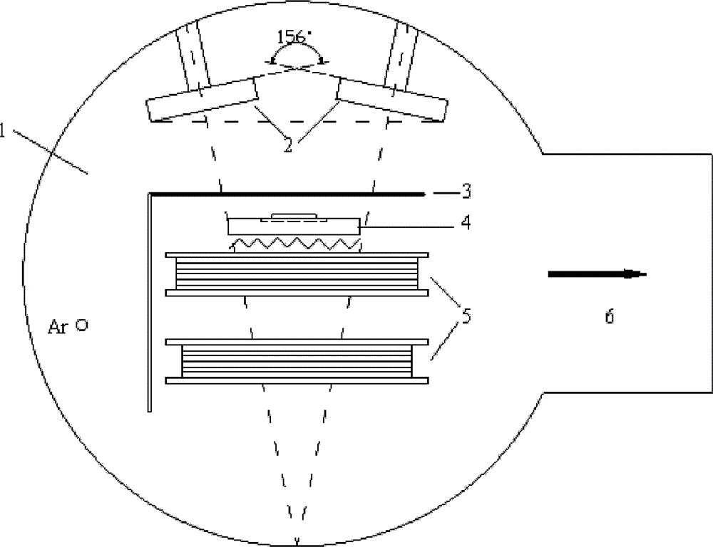
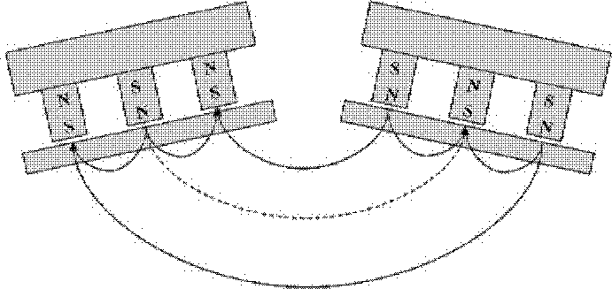
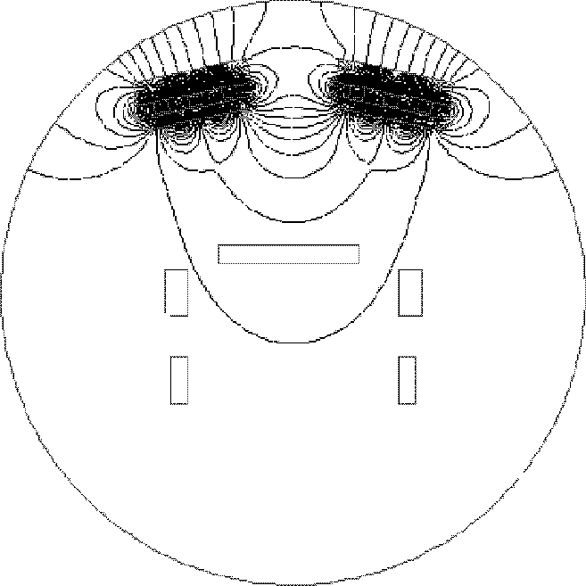
[0050] Pre-evacuation chamber, background vacuum to 1.5×10 -3 Pa, heat the glass substrate to a temperature of 160°C, and at the same time pass in Ar gas to increase the pressure of the vacuum chamber to 1Pa, keep it warm for 30 minutes for desorption, remove impurities physically adsorbed on the surface of the substrate, and facilitate the combination of the film and the substrate, and Nucleation of silicon thin film; then close the Ar gas and re-evacuate the vacuum chamber to 1.5×10 -3Pa, and heat the substrate again, so that the substrate temperature rises to about 500°C; enter Ar gas, the ventilation volume is about 100sccm, when the vacuum chamber pressure rises to 1Pa, turn on the power supply of the silicon target and adjust the voltage to 760V for pre-sputtering , the sputtering time is 30min, which can effectively eliminate the intrinsic oxide layer on the surface. Then keep the vacuum chamber pressure constant, adjust the target power supply and electromagnetic coil...

Embodiment 2

[0053] Pre-evacuation chamber, background vacuum to 1.6×10 -3 Pa, heat the copper-coated glass substrate to a temperature of 160°C, and at the same time pass in Ar gas to raise the pressure of the vacuum chamber to 1Pa, keep it warm for 30 minutes for desorption, remove impurities physically adsorbed on the surface of the substrate, and facilitate the combination of the film and the substrate , and the nucleation of the silicon film; then the Ar gas was turned off, and the vacuum chamber was re-evacuated to 1.5×10 -3 Pa, and heat the substrate again, so that the substrate temperature rises to about 490°C; enter Ar gas, the ventilation rate is 100sccm, when the vacuum chamber pressure rises to 1Pa, turn on the silicon target power supply, adjust the voltage to 760V for pre-sputtering, The sputtering time is 30min, which can effectively eliminate the intrinsic oxide layer on the surface. Then adjust the vacuum chamber pressure to 0.6Pa, adjust the target power supply and the el...

Embodiment 3

[0057] Pre-evacuation chamber, background vacuum to 1.5×10 -3 Pa, heat the glass substrate to a temperature of 160°C, and at the same time pass in Ar gas to increase the pressure of the vacuum chamber to 1Pa, keep it warm for 30 minutes for desorption, remove impurities physically adsorbed on the surface of the substrate, and facilitate the combination of the film and the substrate, and Nucleation of silicon thin film; then close the Ar gas and re-evacuate the vacuum chamber to 1.5×10 -3 Pa, and heat the substrate again, so that the temperature of the substrate rises to about 540 ° C; enter Ar gas, the gas flow is 80s ccm, when the pressure of the vacuum chamber rises to 0.6 Pa, turn on the power supply of the silicon target and adjust the voltage to 760V for pre-sputtering Sputtering, the sputtering time is 30min, which can effectively eliminate the intrinsic oxide layer on the surface. Then keep the vacuum chamber pressure constant, adjust the target power supply and the el...


PUM

PropertyMeasurementUnit
thermal conductivityaaaaaaaaaa

Abstract

The invention relates to the silicon film material preparation filed, and concretely relates to a method for preparing a nanometer silicon film through an intermediate-frequency magnetron sputtering process, and its special device. The method comprises the following steps: sputtering non-equilibrium state twin magnetron silicon targets forming a coupling magnetic field with an applied solenoid by adopting an intermediate-frequency power supply to excite a plasma through utilizing the intermediate-frequency magnetron sputtering process; depositing a nanometer silicon film on a substrate, wherein sputtering of an Ar gas is adopted, the pressure is measured by an ionization gauge, the pressure is controlled between 0.2 and 1.5 in the whole deposition process, the current of the applied solenoid is 0-6A, and the deposition time is 30-90min; evacuating a vacuum chamber to 10<-3>-10<-4>Pa through adopting a vacuum pump group; and heating the substrate to 400-500DEG C to obtain the nanometer silicon film. In the invention, the applied solenoid is adopted to continuously adjust the nonequilibrium degrees of the twin targets, so high-rate ion auxiliary deposition of the nanometer silicon film under low power is realized, the crystal structure of the film is controllable in a large range, and the optical band gap is adjustable.

Description

technical field [0001] The invention relates to the field of preparation of silicon thin film materials, in particular to a method for preparing a nanometer silicon thin film by an intermediate frequency magnetron sputtering method and a special device thereof. Background technique [0002] Today, with the rapid development of solar cell technology, in order to reduce the consumption of silicon materials and reduce the cost of solar cells, thin-film solar cells with silicon thin film as the key material have shown their unique charm. The photosensitive material (silicon thin film) used for silicon thin film solar cells is usually only a few microns thick, which can save a lot of high-purity silicon materials. In addition, its manufacturing process is simple, it consumes less energy, it can be produced continuously in a large area, and low-cost materials such as glass or stainless steel can be used as substrates, and it also has the characteristics of good weak light response...

Claims


Application Information

Patent Timeline
Patent Type & Authority Patents(China)
IPC IPC(8): C23C14/35C23C14/14B82Y40/00B82Y30/00
Inventor 肖金泉高俊华闻立时张林石南林宫骏孙超
Owner INST OF METAL RESEARCH - CHINESE ACAD OF SCI
Why Eureka
Try Eureka