Double-strain plane BiCMOS (Bipolar Complementary Metal-Oxide-Semiconductor Transistor) integrated device and preparation method

An integrated device, double-strain technology, applied in semiconductor/solid-state device manufacturing, electric solid-state devices, semiconductor devices, etc., can solve the problems of confinement, low carrier material mobility of Si materials, etc.

Inactive Publication Date: 2014-12-31
XIDIAN UNIV
View PDF2 Cites 0 Cited by
  • Summary
  • Abstract
  • Description
  • Claims
  • Application Information

AI Technical Summary

Problems solved by technology

[0008] Due to the low mobility of Si material carrier materials, the performance of integrated circuits manufactured using Si BiCMOS technology, especially the frequency performance, is greatly limited; for SiGe BiCMOS technology, although SiGe HBT is used for bipolar transistors, However, Si CMOS is still used for unipolar devices that restrict the improvement of the frequency characteristics of BiCMOS integrated circuits, so these limit the further improvement of the performance of BiCMOS integrated circuits

Method used


Image

  • Double-strain plane BiCMOS (Bipolar Complementary Metal-Oxide-Semiconductor Transistor) integrated device and preparation method

Examples


Embodiment 1

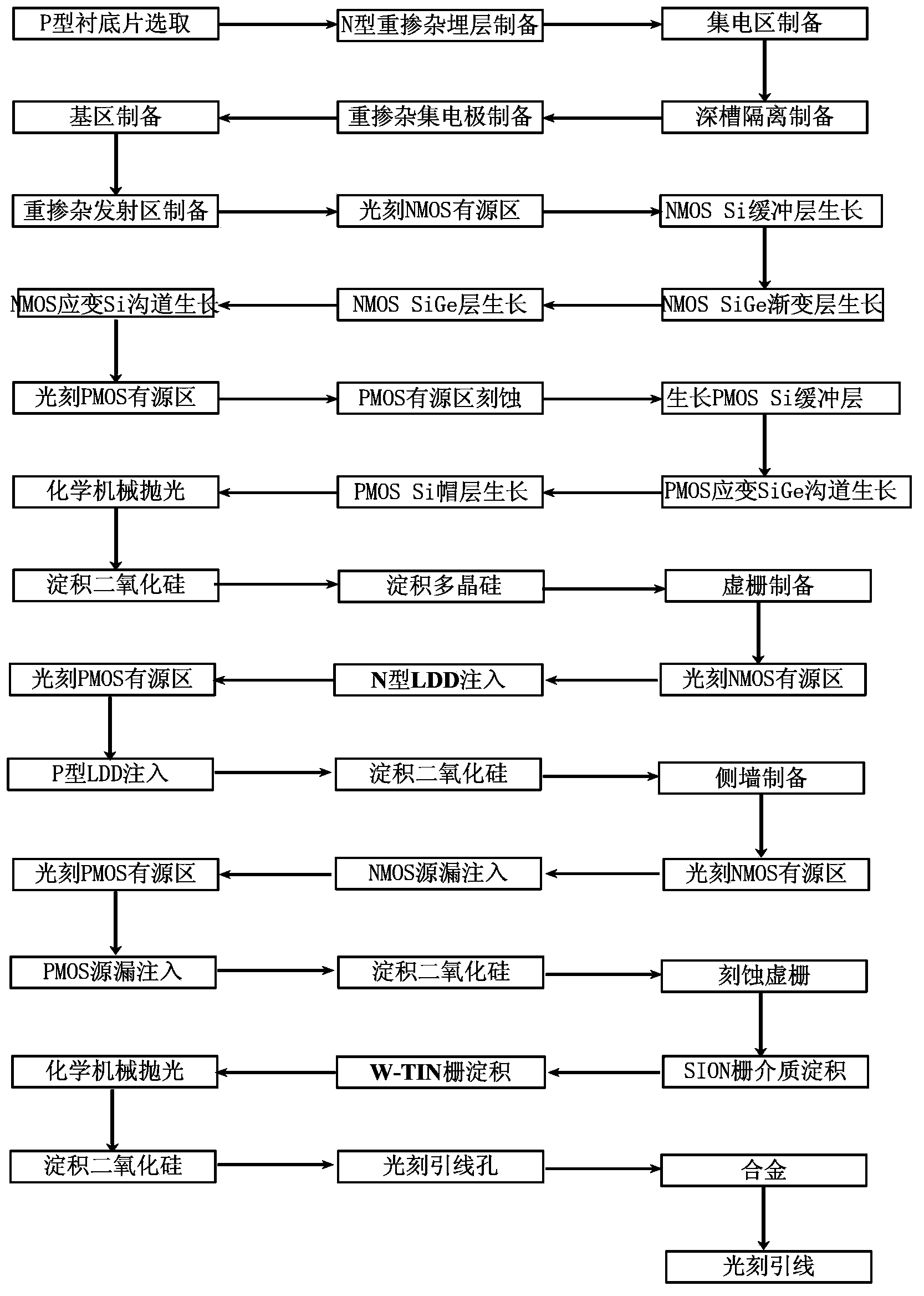
[0096] Embodiment 1: preparation of a dual-strained plane BiCMOS integrated device and circuit with a conduction channel of 45nm,

[0097] Specific steps are as follows:

[0098] Step 1, epitaxial growth.

[0099] (1a) Select the doping concentration to be 5×10 14 cm -3 A P-type Si sheet as a substrate;

[0100] (1b) Thermally oxidize a layer of SiO with a thickness of 300nm on the substrate surface 2 layer;

[0101] (1c) Photoetching the buried layer region, implanting N-type impurities into the buried layer region, and annealing at 800° C. for 90 minutes to activate the impurities to form an N-type heavily doped buried layer region.

[0102] Step 2, isolation area preparation.

[0103] (2a) Remove the excess oxide layer on the surface, and epitaxially grow a layer with a doping concentration of 1×10 16 cm -3 The Si layer, with a thickness of 2 μm, serves as the collector area;

[0104] (2b) Thermally oxidize a layer of SiO with a thickness of 300nm on the substrate ...

Embodiment 2

[0147] Embodiment 2: Preparation of a dual-strained plane BiCMOS integrated device and circuit with a conductive channel of 30nm,

[0148] Specific steps are as follows:

[0149] Step 1, epitaxial growth.

[0150] (1a) Select the doping concentration as 1×10 15 cm -3 A P-type Si sheet as a substrate;

[0151] (1b) Thermally oxidize a layer of SiO with a thickness of 400nm on the substrate surface 2 layer;

[0152] (1c) Photoetching the buried layer region, implanting N-type impurities into the buried layer region, and annealing at 900° C. for 60 minutes to activate the impurities to form an N-type heavily doped buried layer region.

[0153] Step 2, isolation area preparation.

[0154] (2a) Remove the excess oxide layer on the surface, and epitaxially grow a layer with a doping concentration of 5×10 16 cm -3 A Si layer with a thickness of 2.5 μm acts as a collector area;

[0155] (2b) Thermally oxidize a layer of SiO with a thickness of 400nm on the surface of the subs...

Embodiment 3

[0198] Embodiment 3: preparation of a dual-strained plane BiCMOS integrated device and circuit with a conductive channel of 22nm,

[0199] Specific steps are as follows:

[0200] Step 1, epitaxial growth.

[0201] (1a) Select the doping concentration to be 5×10 15 cm -3 A P-type Si sheet as a substrate;

[0202] (1b) Thermally oxidize a layer of SiO with a thickness of 500nm on the surface of the substrate 2 layer;

[0203] (1c) Photoetching the buried layer region, implanting N-type impurities into the buried layer region, and annealing at 950° C. for 30 minutes to activate the impurities to form an N-type heavily doped buried layer region.

[0204] Step 2, isolation area preparation.

[0205] (2a) Remove the excess oxide layer on the surface, and epitaxially grow a layer with a doping concentration of 1×10 17 cm -3 The Si layer, with a thickness of 3 μm, serves as the collector area;

[0206] (2b) Thermally oxidize a layer of SiO with a thickness of 500nm on the sub...


PUM


Abstract

The invention discloses a double-strain plane BiCMOS (Bipolar Complementary Metal-Oxide-Semiconductor Transistor) integrated device and a preparation method. The preparation method comprises the steps of: preparing a buried layer on a substrate piece; preparing a normal Si bipolar transistor in a bipolar device area; etching a deep slot in an active area of the integrated device, and epitaxially growing a P type Si layer, an SiGe gradient layer, an SiGe layer, a strain Si layer as an active area of an NMOS (N-channel metal oxide semiconductor) device and an N type Si layer, a strain SiGe layer, and an Si cap layer as an active area of a PMOS (P-channel metal oxide semiconductor) device; preparing a virtual grid and carrying out light dope source drain injection on the device, depositing SiO2 and self-aligning to form a source drain of the device, depositing an SiON grid dielectric layer and a W-TiN composite grid, and finally forming the double-strain plane BiCMOS integrated device. The method effectively improves the performance of the BiCMOS integrated device and the circuit by using tensile strain Si with high electronic mobility and compressive strain SiGe with high hole mobility as conductive channels of the integrated device respectively.

Description

technical field [0001] The invention belongs to the technical field of semiconductor integrated circuits, and in particular relates to a double strain plane BiCMOS integrated device and a preparation method. Background technique [0002] The integrated circuit, which appeared in 1958, is one of the most influential inventions of the 20th century. Microelectronics, which was born based on this invention, has become the basis of existing modern technology and is accelerating the process of knowledge and informationization of human society. At the same time It has also changed the way of thinking of human beings. It not only provides human beings with a powerful tool to transform nature, but also opens up a broad space for development. [0003] Semiconductor integrated circuits have become the basis of the electronics industry, and people's huge demand for the electronics industry has prompted the rapid development of this field. In the past few decades, the rapid development ...

Claims


Application Information

Patent Timeline
Patent Type & Authority Patents(China)
IPC IPC(8): H01L27/06H01L21/8249
Inventor 张鹤鸣王斌宣荣喜胡辉勇宋建军舒斌王海栋郝跃
Owner XIDIAN UNIV
Why Eureka
Try Eureka